The year 2030 is rapidly approaching, and with it comes advancements in technology that will revolutionize the way we live and work. One of the most significant developments in this field is the introduction of IC PCB layout, which promises to bring about a host of benefits to industries across the board.
IC PCB layout refers to the process of designing and manufacturing integrated circuits (ICs) and printed circuit boards (PCBs) using advanced software and hardware. This technology has the potential to significantly reduce the size and weight of electronic devices, while also increasing their efficiency and performance.
In addition to its impact on the electronics industry, IC PCB layout is also expected to have far-reaching implications for fields such as healthcare, transportation, and energy. With the ability to create smaller and more powerful devices, medical professionals will be able to diagnose and treat patients more accurately and efficiently. Meanwhile, the automotive industry is set to benefit from the increased use of ICs and PCBs in the development of self-driving cars and other advanced technologies.
Overview
What is 2030 IC PCB Layout?
2030 IC PCB Layout is a type of printed circuit board (PCB) layout that is designed to accommodate the latest Integrated Circuit (IC) technology. It is a design approach that takes into account the unique requirements of the ICs that are used in modern electronic devices. This layout is specifically designed to provide the necessary connections and power supply to the ICs, ensuring optimal performance.
Why is 2030 IC PCB Layout Important?
The importance of 2030 IC PCB Layout cannot be overstated. With the rapid advancement of technology, electronic devices are becoming more complex and powerful. This means that the ICs used in these devices are also becoming more complex and require more power. The 2030 IC PCB Layout is designed to provide the necessary power and connections to these ICs, ensuring that they perform optimally.
Moreover, the 2030 IC PCB Layout is important because it allows for the efficient use of space on the PCB. With the increasing complexity of electronic devices, space is becoming a valuable commodity. The 2030 IC PCB Layout ensures that the PCB is designed in a way that maximizes the use of available space, while still providing the necessary connections and power supply to the ICs.
In summary, the 2030 IC PCB Layout is a critical design approach that ensures the optimal performance of modern electronic devices. It takes into account the unique requirements of the latest IC technology and provides the necessary connections and power supply to these ICs. It is an important design approach that allows for the efficient use of space on the PCB.
Key Components
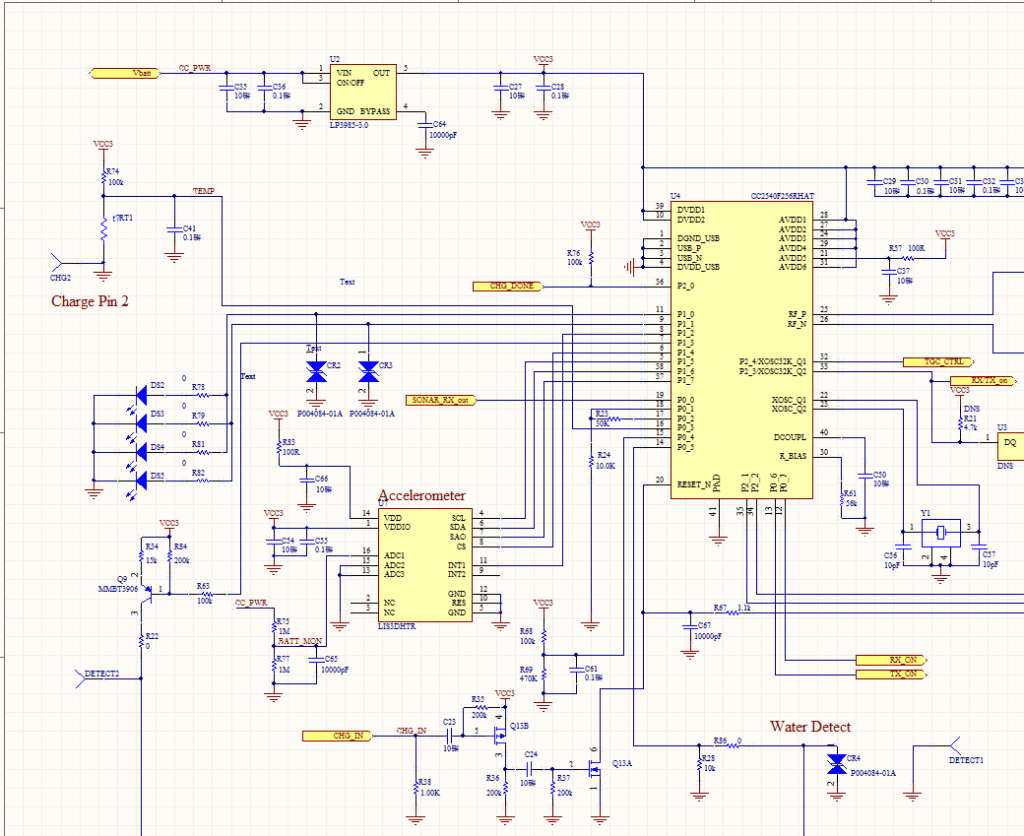
Integrated Circuits (ICs)
Integrated circuits (ICs) are the backbone of any electronic device. They are tiny components that contain multiple electronic circuits on a single chip. ICs can perform a variety of functions, from amplifying signals to processing data. They are used in a wide range of electronic devices, from smartphones to medical equipment.
ICs come in different shapes and sizes, and their functionality varies depending on the application. Some of the most common types of ICs include:
- Microprocessors: These are the brains of a computer or other electronic device. They can perform a variety of functions, from basic arithmetic to complex algorithms.
- Memory chips: These store data and instructions for the device to execute.
- Power management ICs: These regulate the power supply to the device, ensuring that it operates within safe limits.
- Amplifiers: These increase the strength of a signal, making it easier to transmit over long distances.
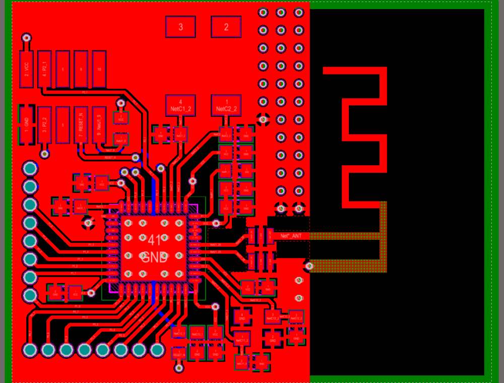
Printed Circuit Boards (PCBs)
Printed circuit boards (PCBs) are the foundation of any electronic device. They are thin boards made of insulating material, with conductive pathways etched onto their surface. These pathways connect the various components of the device, allowing them to communicate with each other.
PCBs are used in a wide range of electronic devices, from simple calculators to complex medical equipment. They come in different sizes and shapes, depending on the application. Some of the key components of a PCB include:
- Copper traces: These are the pathways that connect the various components of the device.
- Solder: This is used to attach the components to the PCB.
- Resistors and capacitors: These components are used to regulate the flow of electricity through the device.
- Diodes: These allow electricity to flow in only one direction, preventing damage to the device.
In summary, ICs and PCBs are two key components of any electronic device. They work together to ensure that the device operates efficiently and reliably. By understanding the role of these components, engineers can design better electronic devices that meet the needs of consumers.
Design Considerations

When designing a PCB layout for an IC, there are several important considerations to keep in mind. These include signal integrity, power distribution network, and thermal management.
Signal Integrity
Signal integrity is crucial in ensuring that the IC functions properly. To achieve good signal integrity, it is important to minimize noise and interference. This can be achieved by:
- Properly routing high-speed signals
- Keeping signal traces short and direct
- Properly terminating transmission lines
- Using ground planes to minimize noise
Power Distribution Network
The power distribution network is responsible for supplying power to the IC and ensuring that it operates within its specified voltage range. To ensure good power distribution, it is important to:
- Use multiple power planes for different voltage levels
- Place decoupling capacitors close to the IC to minimize noise
- Ensure that the power planes are properly connected to the IC
Thermal Management
Thermal management is important to prevent the IC from overheating and malfunctioning. To ensure good thermal management, it is important to:
- Use thermal vias to dissipate heat
- Ensure that the IC is properly connected to a heat sink
- Place the IC in an area with good airflow
By considering these design considerations, you can ensure that your PCB layout for an IC is optimized for performance and reliability.
Tools and Software
PCB Design Software
PCB design software is an essential tool for designing PCBs. It allows designers to create and edit schematics, layout components, and route traces. Some popular PCB design software options include Altium Designer, Eagle PCB, KiCad, and OrCAD.
Each software has its own unique features and capabilities. For example, Altium Designer is known for its user-friendly interface and advanced simulation tools, while Eagle PCB is popular for its affordability and ease of use. KiCad is an open-source software that is free to use and has a large community of users who contribute to its development.
Simulation Tools
Simulation tools are used to test and verify the functionality of a PCB design before it is manufactured. This helps to ensure that the design will work as intended and can save time and money in the long run. Some popular simulation tools include LTSpice, PSpice, and Simulink.
LTSpice is a free, easy-to-use simulation tool that is widely used in the industry. PSpice is a more advanced simulation tool that is popular for its accuracy and extensive library of models. Simulink is a simulation tool that is commonly used for system-level simulations.
Manufacturing Tools
Manufacturing tools are used to prepare the PCB design for production. This includes tools for generating Gerber files, creating BOMs, and generating pick-and-place files. Some popular manufacturing tools include CAM350, CircuitMaker, and PCB123.
CAM350 is a tool that is used to generate Gerber files and perform DFM checks. CircuitMaker is a free tool that is popular for its ease of use and ability to generate BOMs and pick-and-place files. PCB123 is a tool that is used to generate Gerber files and perform DFM checks, and is known for its affordability and ease of use.
Overall, the selection of tools and software for PCB design and manufacturing is vast and varied. It is important to choose the right tools for the job based on the specific needs of the project.
Industry Trends
Miniaturization
The trend towards miniaturization continues to drive the IC PCB layout industry. As electronic devices become smaller and more compact, the demand for smaller and more densely packed PCBs increases. This trend poses a significant challenge for PCB designers who must balance the need for functionality with the limitations of space.
To meet this challenge, designers are turning to advanced technologies such as multi-layer PCBs, smaller components, and innovative routing techniques. The use of smaller components allows for more components to be placed on a single PCB, while multi-layer PCBs increase the number of routing layers available, allowing for more complex designs in a smaller space.
Increased Complexity
As the miniaturization trend continues, the complexity of IC PCB layouts is also increasing. As more components are packed into smaller spaces, the need for precise routing and signal integrity becomes more critical. To meet this challenge, designers are turning to advanced simulation tools that can model the behavior of complex circuits and predict potential problems before they occur.
Additionally, designers are using advanced routing techniques, such as differential pair routing and controlled impedance routing, to ensure signal integrity and reduce noise. These techniques help to ensure that the PCB can handle high-speed signals and maintain reliable communication between components.
IoT Integration
The integration of IoT devices into everyday life is driving the demand for IC PCB layouts that can support the increased connectivity and data processing requirements of these devices. IoT devices require connectivity to the internet, wireless networks, and other devices, which poses a significant challenge for PCB designers.
To meet this challenge, designers are turning to advanced wireless technologies such as Bluetooth and Wi-Fi, as well as innovative power management techniques that can help to extend the battery life of IoT devices. Additionally, designers are incorporating advanced sensors and processors into their designs to enable sophisticated data processing and analysis.
Overall, the trends in IC PCB layout are being driven by the need for smaller, more complex, and more connected devices. To meet these demands, designers are turning to advanced technologies and techniques to create PCBs that can handle the challenges of tomorrow’s electronic devices.
