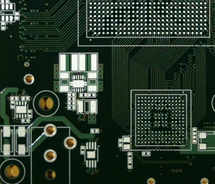
The 8 layer PCB is one of the most popular PCBs in the industry. These boards have unique benefits they offer. Although they have their shortcomings, they are more preferred in the electronics industry. An 8 layer PCB offers all the requirements for signal integrity. In this article, we will discuss how an 8 layer PCB works, the design guidelines, and the prototyping.
What is an 8 Layer PCB Stackup?
An 8 layer PCB is a multilayer board that features four signal layers and four planes that are firmly stacked. These layers include the ground plane, power plane, and signal layers. The ground and power planes separate the signal layers on this PCB. These planes minimize crosstalk between signal layers and also provide inter-plane capacitance. Signal integrity increases due to the arrangement of layers on an 8 layer PCB.
A typical 8 layer PCB stackup offers quality routing space for several power islands. This PCB minimizes the size of complex devices while enhancing working speed. More than four layers of conductive materials are used for the production of an 8 layer PCB. This helps to enhance signal traces; hence, increasing efficiency.
This circuit board is firmly stacked with mutual and reliable connections between all layers. An 8 layer PCB stackup features more planes which helps to increase EMC performance. The extra layers on this PCB stackup also improve routing.
Request 8 Layer PCB Quote, Pls send PCB file to Sales@raypcb.com Now
8 layer Stackup
An 8 layer stackup features four plane layers and four signal layers. Multilayer boards always feature more than two conductive layers; hence one should understand how a stackup works. An 8 layer stackup is the arrangement of insulating layers and conductive layers that make up a board. A good 8 layer stackup will help you deal with signal integrity problems.
For an 8 layer stackup, general layers are signal layers, power plane, and ground plane. Each of these layers plays a significant role in the functionality of a stackup. Layer distribution should conform to a balanced structure in an 8 layer stackup. In this stackup, there are at least one or more prepregs and cores.
The prepregs use high heat to stack the layers firmly into a whole board. The cores are a product of a glass-reinforced epoxy laminate. The thickness of the core varies. Usually, the thickness ranges from 0.1mm to 0.3 mm.
Typical Arrangements on an 8 Layer Stackup
There are different arrangements of planes and signal layers on an 8 layer PCB stackup. These arrangements depend on the intended application requirements. Signal 1 stands for the top layer, Signal 2 and Signal 3 are both inner layers. Signal 4 represents the bottom layer.
Type 1
- Signal 1
- Ground
- Signal 2
- Power
- Ground
- Signal 3
- Power
- Signal 4
As you can see, there are four signal layers, two ground planes, and power planes on this stackup. The power and ground planes separate the signal layers. In this type of stackup, all signal layers have at least one power plane. The ground and power planes offer great inter plane capacitance. If the power islands on your system are close to the bottom layer, they can’t ground capacitance. Furthermore, the return path for the high-speed signals in signal 4 is the power plane.
Type 2
- Signal 1
- Ground
- Signal 2
- Ground
- Power
- Signal
- Ground
- Signal 4
In this type of stackup, the planes are moved to the center. This arrangement helps you have a tightly coupled power and ground plane pair. It is a great arrangement that offers great signal integrity.
Type 3
- Signal 1
- Ground
- Power
- Signal 2
- Signal 3
- Ground
- Power
- Signal 4
This configuration type helps to remove any possible crosstalk between signal 2 and signal 3. Here, the signal layers are all adjacent to planes. The layers are also coupled closely. Signal2 and Signal 3 are both buried between planes. So, the planes can serve as a shield and as such, reducing the emissions from the signal layers. This stackup arrangement features two ground planes, thereby reducing the ground impedance.
Type 4
- Ground
- Signal 1
- Ground
- Signal 2
- Signal 3
- Power
- Signal 4
- Ground
Here, the ground planes serve as the top and bottom layers. There are also three ground planes, of which two are outer layers. In this type of configuration, all routing layers are between planes. This serve as a shield for the routing layers.
Functions of Ground and Power Planes in 8 Layer Stackup
The ground and power planes play a significant role in an 8 layer PCB stackup. The manufacturer must pay proper attention to these planes. The ground plane provides a clear return path on an 8 layer PCB. Without this return path, signals can produce EMI for the board.
The ground and power plane increase the stability of the reference voltages. Almost all components on the circuit board connect to a power net. The return voltage then comes back via the ground net. Wider traces need to be used for routing ground nets. The ground plane makes it easy to connect every component to the ground net.
These planes are also very useful in controlling crosstalk. As there is an increase in signal speeds, digital circuits switch positions. This will cause noise pulses via the ground circuit. Other parts of the circuit might be impacted as a result of this. A ground plane will minimize the amount of noise and interference.
An 8 layer PCB manufacturer can regulate the electrical performance of a circuit with the use of ground planes. Incorporating a ground plane between two signal layers will eliminate crosstalk between them. A power plane and ground plane can improve the signal integrity of a board.
Request 8 Layer PCB Quote, Pls send PCB file to Sales@raypcb.com Now
Tips for 8 Layer PCB Design
Most times, it is believed that an 8 layer PCB provides solutions to all EMI problems. This isn’t true as there are certain checks to put in place. The design of an 8 layer stackup can be a complex one. There are factors that can make a stackup perform less. However, as a PCB designer, your goal is to design a functional stackup. You need to understand that there are some important design techniques that help you achieve a functional 8 layer PCB.
Impedance Control
Impedance control plays a significant role in the success of an 8 layer PCB design. During the PCB design, the designer should measure the impedance of some traces. Impedance control can be achieved by matching the properties of the substrate material with the locations and dimensions of the trace. Ensure that the impedance of the signal of a trace is within the specified value. Impedance control offers great board performance.
Signal shielding
An 8 layer PCB manufacturer must shield the signal layers from one another. This will help prevent signal loss and infractions. This is one of the reasons the 8 layer PCB is mostly preferred. It features more planes that serve as a shield for the signal layers.
Prevention of Noise Decoupling
PCB designers must consider noise decoupling during an 8 layer stackup design. Noise decoupling should be prevented at all costs. Creating a digital ground plane is the best way to prevent it. This digital ground plane will aid the design of multiple ground and power planes. These planes will then be deployed through the stackup.
Layers Balancing
Layer balancing is a gateway to designing a sound PCB stackup. A balanced 8 layer stackup is one that the cross sectional structure and the layer surfaces of the circuit are symmetrical. Designers have to remove areas that could deform due to the stresses of manufacturing processing. Therefore, it is important the PCB manufacturer evaluates the review of the circuit layout.
Important Considerations for an 8 layer Stackup Fabrication
There are certain considerations that will help enhance the functionality of an 8 layer stackup.
Stackup measling
During the fabrication of an 8 layer PCB, manufacturers are likely to encounter this problem. To avoid stackup measling, use silicon pads and epoxy plates while arranging the board. This helps the board’s thickness to be uniform and as well as eliminates measling.
Interlayer offset
It is possible to offset the internal layers of an 8 layer PCB during the fabrication process. Manufacturers can tackle this problem by using rivet dowels methods for the board designs.
Core materials
The core of a multilayer board is base material coated with copper. Some core materials are very difficult to fabricate. Therefore, you should be careful in the choice of your core material.
Bow and Twist
The bow and twist determine the flatness of multilayer boards. The bow and twist problem arises when there is an uneven copper distribution. This can make electrical components and parts of a board to shift during the assembly process. The best remedy is to design and fabricate the layer stackups in a symmetrical way.
How to Choose the Best 8 Layer PCB Manufacturer
The functionality of your 8 layer PCB stackup depends on how it is manufactured. An 8 layer PCB stackup is best designed and manufactured by an expert. There are certain factors you should consider when choosing an 8 layer PCB manufacturer.
Expertise
This involves the skill and experience of the manufacturer. Due to the complexity of 8 layer stackup, you need a skilled and experienced manufacturer. You should ask questions like how long has the manufacturer been doing this? What type of certification does the manufacturer have? The answers to these questions will help you make your decision. The manufacturer should also produce a stackup that meets your requirements.
Turnaround time
This refers to the amount of time required to complete the production of a board. Can your manufacturer complete the design and fabrication of the circuit within the specified time. Ensure that the 8 layer PCB manufacturer offers a feasible turnaround time. You can go through the reviews of the past clients of this manufacturer.
Order capacity
Ensure that the 8 layer PCB manufacturer can deliver any amount of boards you order. Some manufacturers can only deliver circuit boards in small amounts. For people who need to design an 8 layer PCB stackup in large amounts, consider this factor.
Customer service
This is interpreted as availability and responsiveness. You want a manufacturer who is always available to take demands and ensure they are met. An 8 layer stackup manufacturer should also be able to offer advice to its clients.
Why Use an 8 Layer PCB Stackup
An 8 layer PCB offers numerous benefits. The fact that it features four plane layers and four signal layers makes it a better option for most applications. When more plane layers are added to a stackup, they provide better routing. Here are reasons 8 layer PCB stackup is a preferred choice.
Increases signal integrity
An 8 layer PCB stackup increases the signal integrity of a circuit. Incorporating an 8 layer stackup in electronic devices helps to maximize their functionality. The inclusion of multiple ground planes and power planes in this stackup also helps to have a functional board. These plane layers serve as a shield for the other four signal layers; hence, reducing EMI.
Reduces EMI
This stackup is ideal for use in complex devices since it reduces electromagnetic interference. The type of arrangement on an 8 layer stackup can also help to reduce or eliminate radiation.
Reduces cost of operation
This is one of the benefits of an 8 layer stackup. PCB manufacturers depend on this stackup since they reduce the cost of operation. These stackups are very durable and require low maintenance. 8 layer PCBs help to save space on a board.
Conclusion
The manufacturing of an 8 layer PCB stackup is a detailed process that requires a layered approach. An 8 layer stackup is commonly used for the production of most electronic devices. Complex devices feature these stackups since they provide great EMC performance. The extra layers featured by an 8 layer board helps signal routing. The role of this board in today’s electronic industry can’t be overemphasized. An 8 layer PCB manufacturer should design this stackup with functionality and quality in mind.
