When it comes to printed circuit board (PCB) prototyping, precision and attention to detail are critical factors to ensure the successful development of a high-quality product. A PCB is the backbone of any electronic device, and its design can have a significant impact on the device’s overall performance and reliability. With rapid advancements in PCB technology, manufacturers and designers must stay ahead of the curve by understanding and addressing essential aspects of the prototyping process.
In this article, we will discuss eight vital factors to consider during the PCB prototyping stage. These elements are crucial to achieving a seamless transition from concept to functional prototype while minimizing errors, cost overruns, and production delays. The article delves into material selection, design rules, testing procedures, and other critical aspects that impact the quality and efficiency of PCB prototyping efforts.
By incorporating these insights and best practices into your PCB prototyping workflow, you can effectively avoid common pitfalls, optimize your design for manufacturability, and ensure that your electronic devices perform optimally in the hands of end-users. Armed with this knowledge, designers and manufacturers alike can confidently navigate the complex landscape of PCB prototyping and contribute to the design and production of innovative, high-quality electronic products.
Understanding PCB Prototyping
PCB prototyping is the process of creating a preliminary version of a printed circuit board (PCB) to test and verify its functionality before moving to mass production. This crucial step in PCB design helps identify potential issues early in the product development process, saving time, money, and resources.
The first aspect to consider in PCB prototyping is the selection of appropriate materials. Different materials have varying properties in terms of thermal conductivity, electrical performance, and mechanical strength. Some commonly used materials for PCBs are:
- FR-4: A popular choice due to its durability, low cost, and good electrical properties
- Aluminum: Offers excellent thermal conductivity and is suitable for high-power applications
- Rogers: Provides better high-frequency performance and low signal loss compared to FR-4
Another vital factor in successful PCB prototyping is the design for manufacturing (DFM) guidelines. Adhering to DFM principles ensures the manufacturability and assembly of PCBs, minimizing the chances of errors and defects. Important DFM aspects include:
- Trace width and spacing: Ensuring adequate spacing between traces and correct trace width to prevent short circuits and signal interference
- Via size and placement: Proper sizing and positioning of vias to ensure reliable connectivity and prevent manufacturing issues
- Component arrangement: Components need to be adequately spaced, avoiding interference with each other and ensuring PCB assembly efficiency
Testing and verification are also essential in the PCB prototyping process. Having the designs thoroughly tested can prevent potential issues upon manufacturing, such as:
- Electrical testing: Ensuring the functionality and accuracy of the circuit by using inspection tools like flying probe testers
- Mechanical testing: Assessing the mechanical strength and durability of the PCB and its components under stress
- Environmental testing: Evaluating the PCB’s performance under various environmental conditions, such as temperature, humidity, and vibration
Finally, the collaboration between the PCB designer and the manufacturer plays a significant role in the prototyping process. Open communication helps address any issues related to design, material selection, or manufacturing techniques. This collaborative approach ensures that the final product meets the required specifications and reduces manufacturing errors.
Key Design Considerations
Component Selection
Choosing the right components is critical for a successful PCB prototyping process. Factors to consider include:
- Compatibility: Make sure all the components selected are compatible with your design requirements and objectives.
- Availability: Opt for commonly available components to ensure easy sourcing and replacement during the prototyping and manufacturing stages.
- Price: Consider the cost of components to stay within budget.
PCB Material
Selecting the appropriate PCB material can have a significant impact on performance, durability, and cost. Some of the common PCB materials are:
- FR-4: The most widely used material that offers a good balance between performance and cost.
- High-Temperature: Best suited for applications requiring high thermal performance and stability, such as automotive and aerospace systems.
- Flexible: Ideal for designs that need to conform to curved surfaces or flexibility.
Layout Design
A well-designed layout can help reduce noise, improve signal integrity, and increase the overall performance of the PCB. Consider the following aspects:
- Signal routing: Use shorter and fewer signal traces to minimize the risk of signal integrity and electromagnetic interference issues.
- Power distribution: Plan the power supply layout to ensure a stable and low-noise voltage supply to all components.
- Grounding: Implement a proper grounding strategy to reduce noise and interference in the circuit.
By paying attention to these key aspects during PCB prototyping, you can increase the chances of a successful and efficient project outcome.
Manufacturing Process

Panelization
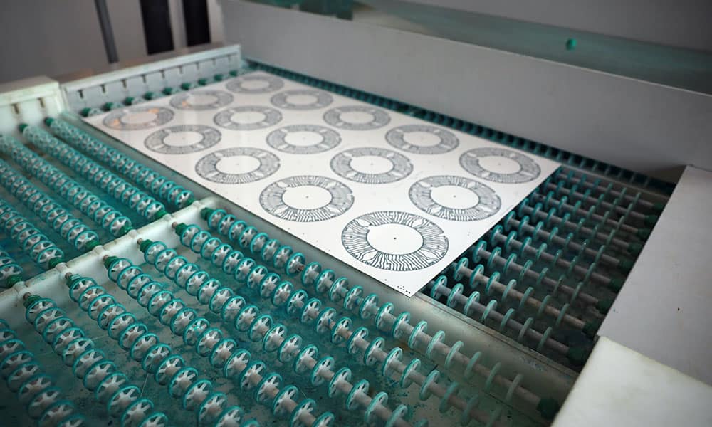
Panelization is a crucial step in the PCB prototyping process, where the individual PCBs are arranged on a larger panel to optimize the manufacturing process. This technique helps reduce waste and increases the production efficiency of the PCBs.
- Optimal panel size: Selecting the right panel size ensures that the maximum number of PCBs are fabricated in a single run without compromising on quality.
- Breakaway methods: Choosing the appropriate method (e.g., v-groove or tab-routing) for separating the individual PCBs ensures a smooth separation without damaging the components.
Drilling
Drilling is a vital PCB manufacturing step, as it creates holes for mounting components and establishes connections between the different layers of a multi-layer PCB.
- Hole size and tolerance: Accurately drilling holes with the correct size and tolerance ensures that components fit properly and connections are established reliably.
- Drill material: The choice of drill material (e.g., carbide or high-speed steel) affects hole quality and efficiency, as different materials have varying wear resistance and cutting speeds.
- Registration accuracy: Achieving precise alignment of drilled holes is essential for ensuring that components can be mounted accurately on the board.
By paying attention to these key factors in the manufacturing process, optimal PCB prototyping results can be achieved, leading to a successful production process.
Importance of Testing and Debugging
Testing and debugging play a crucial role in PCB prototyping, ensuring that the final product functions correctly and meets all requirements. Rigorous testing helps identify potential issues early in the development process, saving time, resources, and frustration.
One important aspect of testing is the use of electrical testing methods, such as continuity testing and insulation resistance testing. Continuity testing verifies that there are no breaks in the electrical paths, while insulation resistance testing ensures that there are no undesired conductive paths between different circuit elements.
Another vital testing methodology is In-Circuit Testing (ICT), where a test fixture is used to check all components on the board for correct function and value. This provides a comprehensive evaluation of the PCB performance under real conditions.
Debugging focuses on tracing and resolving errors or design flaws that might have been missed during the testing phase. The following are a few essential debugging tools and techniques used in PCB prototyping:
- Visual Inspection: A simple yet effective method to detect defects such as misalignments, solder bridge, or missing components.
- X-Ray Inspection: This method helps identify hidden defects such as solder voids, tombstoned components, and insufficient solder joints.
- Automated Optical Inspection (AOI): It uses cameras and software algorithms to inspect PCBs for any inconsistencies or defects, allowing for quick identification of problematic areas.
To summarize, a thorough testing and debugging process is vital in PCB prototyping to ensure reliable, efficient, and high-quality end products. These processes not only save time and resources but also help maintain the integrity of the overall PCB design.
Impact of Component Placement
Component placement is a crucial factor in PCB prototyping as it directly affects the efficiency and performance of your circuit board. Careful consideration must be taken during this stage to ensure optimal functioning and to prevent potential design issues.
Some key considerations during component placement include:
-
Orientation and Alignment: Ensure components are placed with their pins aligned correctly and in a logical direction. This will make it easier to route the signals between components and help reduce the chances of errors during assembly.
-
Thermal Management: Proper placement of components with high thermal dissipation rates is essential to prevent overheating. Place them near the edges or in areas with adequate airflow or heat dissipation features, such as heat sinks.
-
Mechanical Constraints: Always consider the physical limitations of your board, including the availability of space and the presence of other components. Avoid placing delicate components near high-stress areas or those prone to physical damage during assembly or usage.
-
Electromagnetic Interference (EMI): Some components can generate EMI, which may interfere with the performance of other nearby components. Place these components away from sensitive parts, and ensure proper shielding is in place if necessary.
Adhering to the following guidelines can lead to improved PCB prototyping results:
- Group related components together to create a more organized layout and simplify routing.
- Prioritize placing components that require specific space and orientation, such as connectors and larger components, before moving to smaller components.
- Keep the power supply and ground paths as short as possible to reduce noise and improve the overall stability of your circuit.
- Minimize signal path lengths to reduce potential issues with signal integrity, crosstalk, and EMI.
Taking the time to thoroughly plan your component placement during the PCB prototyping process can drastically improve the overall functionality and reliability of your finished product. Keep these factors in mind to ensure a successful prototype and a smoother transition to the manufacturing stage.
Preventing Common Errors
Solder Mask Mishaps
Solder mask, an important element for protecting and insulating PCB traces, can sometimes lead to errors. To avoid these issues, ensure the mask’s design meets manufacturer specifications. Particularly, verify the minimum trace, space, and pad sizes. Additionally, double-check the mask size and any openings, as incorrect designs could cause shorts or poor connections.
Insufficient Copper Clearance
Insufficient copper clearance can lead to issues, such as short circuits and poor signal integrity. To prevent this problem, follow the guidelines for minimum clearance distances between copper features (traces, pads, and vias). Abiding by these rules will maintain reliable connections and improve overall board performance.
- Stick to the manufacturer’s recommended clearances to prevent issues.
- Use the correct unit of measurement while designing the PCB layout.
By adhering to these guidelines, you can minimize common errors that impact PCB prototyping and improve the overall efficiency of your design process.
Conclusion
In this article, we discussed the 8 important matters to consider during PCB prototyping. By taking these factors into account, you can ensure a successful prototype and an efficient development process.
We covered the significance of board materials and layout, which have a direct impact on PCB performance. These aspects determine not only the manufacturability of your PCB but also its functionality, reliability, and cost.
Moreover, managing power distribution, component placement, and routing decisions plays a crucial role in maximizing circuit efficiency and minimizing noise or interference in the design.
Finally, we emphasized the benefits of simulation, proper documentation, and communication during the prototyping phase. These practices help in identifying potential issues early on, reducing the need for time-consuming and costly revisions.
By keeping these 8 matters in mind and applying them during the PCB prototyping phase, you are more likely to achieve a successful final product and improve the overall development experience.
