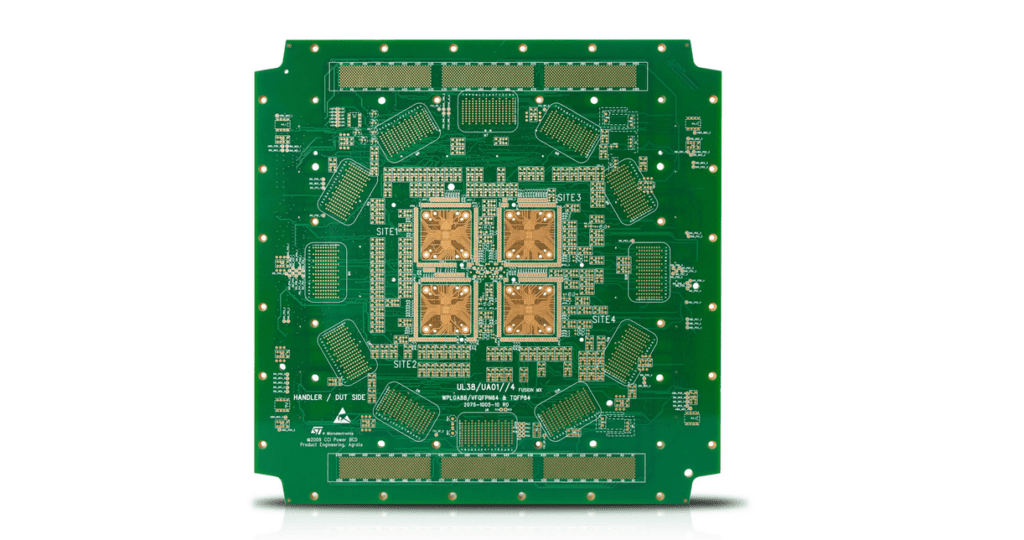
Altium 4 layer PCBs are becoming increasingly popular in the electronics industry due to their numerous benefits. These PCBs consist of four layers of conductive material separated by insulating layers, which allows for more complex circuitry and higher density designs. This technology has revolutionized the way electronic devices are designed and manufactured.
One of the main advantages of Altium 4 layer PCBs is their ability to reduce the size of electronic devices. With more layers available for routing, designers can create smaller and more compact devices without sacrificing functionality. This is particularly important in industries such as aerospace and medical, where space is at a premium.
Another benefit of Altium 4 layer PCBs is their improved signal integrity. By separating power and ground planes from signal layers, designers can reduce the risk of signal interference and crosstalk. This results in more reliable and efficient electronic devices. Overall, Altium 4 layer PCBs offer a cost-effective and efficient solution for creating high-performance electronic devices with complex circuitry.
Benefits
Altium 4 layer PCBs offer several benefits over traditional 2 layer PCBs. Here are a few of the main advantages:
1. Increased Design Flexibility
4 layer PCBs provide more routing options, which makes it easier to design complex circuits. With more layers, designers can create more intricate connections and layouts, which can lead to better performance and reliability.
2. Improved Signal Integrity
The additional layers in a 4 layer PCB can help reduce electromagnetic interference (EMI) and crosstalk between signals. This can result in improved signal integrity and reduced noise, which can lead to better overall performance.
3. Higher Component Density
4 layer PCBs can accommodate more components in a smaller space. This can be especially useful for designs that require a high level of functionality in a compact form factor.
4. Better Thermal Management
The additional layers in a 4 layer PCB can also help with thermal management. By adding power and ground planes, designers can create a more efficient heat dissipation system, which can help prevent overheating and improve the overall reliability of the circuit.
In summary, Altium 4 layer PCBs offer increased design flexibility, improved signal integrity, higher component density, and better thermal management. These benefits make them an excellent choice for a wide range of applications, from consumer electronics to industrial control systems.
Design Considerations
When designing a 4 layer PCB with Altium, there are several factors to consider. These include the board size, the number and type of components, and the signal integrity requirements.
Firstly, the board size should be carefully considered. Larger boards will require more layers to accommodate all the necessary components, while smaller boards may be able to function with fewer layers. It is important to strike a balance between board size and layer count to ensure the most efficient design.
Secondly, the number and type of components will also impact the design. High-density designs with many components will require more layers to accommodate all the necessary traces and vias. Additionally, the type of components used will affect the signal integrity requirements, and therefore the layer count.
Finally, signal integrity is a critical consideration when designing a 4 layer PCB with Altium. Proper trace routing and impedance control are necessary to ensure that signals are transmitted accurately and without interference. Careful placement of components and vias can also help to minimize signal noise and crosstalk.
Overall, designing a 4 layer PCB with Altium requires careful consideration of board size, component count, and signal integrity requirements. By taking these factors into account, designers can create efficient and effective PCB designs that meet their specific needs.
Layer Stackup

The layer stackup is an essential aspect of the design of a 4-layer PCB. It is the arrangement of the layers in the PCB, and it determines the electrical and mechanical properties of the board. The layer stackup is critical in determining the performance of the PCB as it affects the signal integrity, power integrity, and electromagnetic compatibility of the board.
The layer stackup is typically composed of four layers: two signal layers, one power plane, and one ground plane. The signal layers are the top and bottom layers, and they carry the signals that connect the components on the board. The power plane is a layer that carries the power supply to the components, while the ground plane is a layer that provides a low impedance path for the return current.
The layer stackup is designed to minimize the electromagnetic interference (EMI) and crosstalk between the signal traces. The power plane and ground plane are placed between the signal layers to provide shielding and reduce EMI. The thickness and spacing of the layers are also optimized to minimize the crosstalk between the signal traces.
The layer stackup also affects the mechanical properties of the board. The thickness and spacing of the layers determine the overall thickness of the board, and they also affect the flexibility and rigidity of the board. The layer stackup is designed to balance the electrical and mechanical properties of the board to ensure optimal performance.
In conclusion, the layer stackup is a critical aspect of the design of a 4-layer PCB. It determines the electrical and mechanical properties of the board and affects the performance of the PCB. The layer stackup is designed to optimize the signal integrity, power integrity, and electromagnetic compatibility of the board while balancing the mechanical properties of the board.
Traces and Routing
When designing a 4-layer PCB using Altium, it is important to consider the trace width and spacing. These values will depend on the current carrying capacity and the voltage level of the circuit. Altium provides a set of default trace widths and spacing values, but they can be customized based on the specific requirements of the circuit.
Routing is a crucial aspect of PCB design, and Altium makes it easy to route traces between components. The software provides a variety of routing tools, including interactive routing and auto-routing. Interactive routing allows the designer to manually route traces, while auto-routing automatically generates the routing based on the design rules.
Altium also offers a range of routing options, such as differential pairs, length matching, and high-speed routing. Differential pairs are used for high-speed data transmission, and Altium provides tools to ensure that the pairs are routed correctly. Length matching is important for signals that need to arrive at the same time, and Altium provides tools to help achieve this. High-speed routing is used for signals that require fast transmission, and Altium offers a range of options to optimize the routing.
Overall, Altium provides a range of tools and options to help designers create high-quality 4-layer PCBs with accurate and efficient traces and routing.
Ground and Power Planes
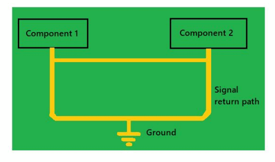
One of the key advantages of using a 4-layer PCB design in Altium is the ability to include dedicated ground and power planes. These planes are large areas of copper that are connected to ground or power respectively, and are located on internal layers of the PCB.
By including these planes, you can greatly improve the overall performance and reliability of your design. Here are some of the benefits:
-
Reduced noise: Ground planes provide a low-impedance path for noise to flow to ground, which reduces the amount of noise that can couple onto signal traces.
-
Improved signal integrity: Power planes provide a stable voltage source, which helps to reduce voltage drop and improve signal integrity.
-
Increased thermal dissipation: Power planes can also act as heat sinks, helping to dissipate heat from power-hungry components.
When designing ground and power planes, it’s important to consider the following:
-
Plane size: The larger the plane, the better the performance. However, you also need to consider the available space on your PCB and the manufacturing capabilities of your PCB manufacturer.
-
Plane spacing: The distance between the ground and power planes can affect their performance. Ideally, you want to keep the spacing as small as possible to reduce noise and improve signal integrity.
-
Plane connections: The ground and power planes should be connected to the rest of the circuit using vias. Make sure that there are enough vias to provide a low-impedance connection.
In Altium, you can easily add ground and power planes to your design by creating a new internal layer and assigning it to the appropriate net. You can then use the Polygon Pour feature to create the plane. Make sure to follow the guidelines above to ensure that your planes are optimized for performance and reliability.
