Altium reuse PCB layout is a powerful tool that can save time, effort, and money for electronic designers. By reusing PCB layouts from previous designs, designers can avoid the time-consuming process of creating new layouts from scratch. This can be especially helpful when designing complex electronic systems that require multiple PCBs.
Altium reuse PCB layout is a feature that is available in Altium Designer, a popular software tool used by electronic designers. With this feature, designers can easily reuse existing PCB layouts and make modifications as needed for the current design. This can be a huge time-saver, especially for designs that have similar components or layouts. Additionally, Altium Designer has a library of pre-designed components that can be easily added to new designs, further streamlining the design process.
Overview
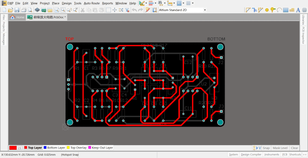
What is Altium Reuse PCB Layout?
Altium Reuse PCB Layout is a feature that allows engineers to reuse existing PCB designs in new projects. This feature saves time and effort by allowing engineers to easily import existing designs and modify them to meet the requirements of new projects. With Altium Reuse PCB Layout, engineers can easily copy and paste existing designs, or import them directly from other projects.
Benefits of Altium Reuse PCB Layout
Altium Reuse PCB Layout offers several benefits to engineers, including:
- Time savings: Engineers can save time by reusing existing designs instead of starting from scratch.
- Consistency: Reusing existing designs can help ensure consistency across projects.
- Cost savings: Reusing existing designs can help reduce the cost of development.
- Improved quality: Reusing existing designs can help improve the quality of the final product by leveraging proven designs.
Overall, Altium Reuse PCB Layout is a powerful tool that can help engineers save time, reduce costs, and improve the quality of their designs.
How to Reuse PCB Layout in Altium
Step 1: Open the PCB Project
To reuse a PCB layout in Altium, you must first open the existing PCB project. This can be done by clicking on the “Open Project” button in the “Projects” panel. Once the project is open, you will be able to access the PCB layout and components.
Step 2: Create a Blank PCB Project
Next, create a new blank PCB project by clicking on the “New PCB Project” button in the “Projects” panel. This will open a new project with a blank PCB layout.
Step 3: Import the Existing PCB Project
To import the existing PCB project, click on the “File” menu and select “Import.” Choose the PCB project file that you want to reuse and click “Open.” The existing PCB layout and components will now be imported into the new project.
Step 4: Reuse PCB Layout and Components
Now that the existing PCB layout and components have been imported, you can begin reusing them in your new project. To reuse the layout, simply copy and paste it into the new project. To reuse the components, you can either copy and paste them or add them to the new project’s component library.
By following these simple steps, you can easily reuse a PCB layout in Altium and save time on your next project.
Best Practices for Altium Reuse PCB Layout

Use Consistent Design Rules
When reusing PCB layouts in Altium, it’s important to maintain consistency in your design rules. This means using the same PCB layer stackup, trace widths, and via sizes across all designs. Inconsistent design rules can lead to manufacturing errors and signal integrity issues.
To ensure consistency, create a design rule template that includes all the necessary design rules for your project. This template can be applied to all new designs, ensuring that all designs adhere to the same rules.
Organize Your Libraries
Organizing your libraries is crucial for efficient reuse of PCB layouts. All components used in your designs should be stored in a central library. This library should be organized in a way that makes it easy to find and reuse components.
Use descriptive names for your libraries and components, and include all relevant information, such as part numbers and datasheets. Create separate libraries for each type of component, such as resistors, capacitors, and ICs.
Create a Master Project Template
Creating a master project template is an effective way to streamline the reuse of PCB layouts in Altium. This template should include all the necessary design files, libraries, and design rule templates.
By using a master project template, you can quickly create new projects that adhere to the same design rules and use the same components as previous designs. This saves time and ensures consistency across all designs.
In conclusion, following these best practices for Altium reuse PCB layout can help ensure consistency, efficiency, and accuracy in your designs.
Conclusion
In conclusion, Altium Reuse PCB Layout is a powerful tool for designers who want to save time and effort in their projects. By utilizing the reuse feature, designers can easily copy and paste existing layout designs, making it easier to create new designs and reduce the risk of errors.
Additionally, Altium Reuse PCB Layout allows designers to create templates for frequently used designs, further streamlining the design process. With the ability to customize templates, designers can ensure that all designs meet their specific requirements and standards.
Overall, Altium Reuse PCB Layout is a valuable tool for designers looking to improve their efficiency and productivity. With its intuitive interface and powerful features, designers can easily create and modify designs, saving time and effort in the process.
