Today, castellated holes have gained much popularity, and have become more common. This is happening due to the great development in the high-tech industries. Designers present in the castellated circuit board industry must have a great comprehension of what castellated hoes are. What’s their importance? And how are they designed?
Here, you will learn the significance of castellated homes and their usefulness in the production of PCBs. In addition, you will also know how best to go about castellated PCBs accurately and quickly. Please continue reading to have a deep understanding on how to utilize castellated holes for your POCB production.
What are Castellated Holes?
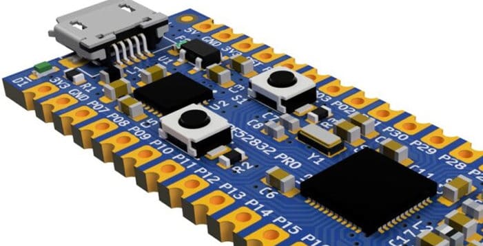
Castellated holes can also be referred to as castellations or plated half holes. These are indentations that are created like semi-plated holes present on PCB boards’ edges. With these castellations, mounting a PCB board right on top of a second one during assembly comes easy.
With respect to the application, rather than half holes, it may seem like a larger or small fraction of the broken circle. The design of these holes is made to offer the best alignment between your boards during soldering.
The process of mounting occurs with assistance from board-to-board soldering and castellated holes. The creation of castellated holes is done by different modules of PCB, either Wi-Fi or Bluetooth modules. Each module may serve as an independent part that is mounted onto a different board all through the process of assembly.
SMT (Surface Mount Technology) and THT (Through Hole Technology) are usually utilized during the process of PCB assembly. Asides from these, the board-to-board type of soldering is utilized whenever you want to mount one board on the other. Castellations act as a sort of link in-between the board and the module onto which you can solder the module.
Request Castellated PCB Quote, Pls Send PCB Files to Sales@raypcb.com Now
How to Form Castellated Holes
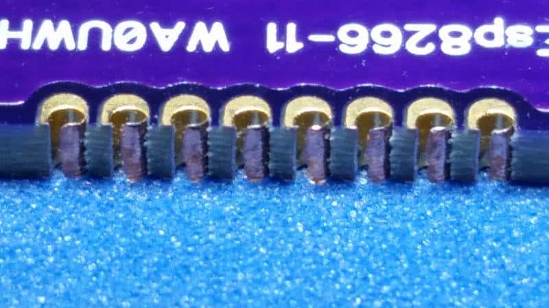
Forming or creating castellated holes isn’t a big deal. The process is a straightforward one. This creation deals with the drilling and the copper plating of the full holes in the castellated circuit board. This involves the cutting of the top spot into halves. This forms half or partial holes on the PCB edge.
Why is the Use of Castellated Holes Important?
When you create castellated holes on your board’s edges, you can use them to replicate some parts of your PCB circuit. For example, if you have a circuit including a filter, feedback loops, or an inverter. You can mass-produce these little sub-circuits, test and solder them onto your main PCB, which contains the circuit’s remaining parts where needed.
The following are the uses of castellated holes.
- You can use a castellated PCB as a breakout board for a specific portion of your larger PCB.
- With castellated holes, you can easily change the component’s Pin layout with respect to user requirements.
- You can produce integrated modules on one PCB board making use of a castellationthat can be further utilized into a different assembly while production is on.
- It is easy to mount PCBs having castellated holes to a second PCB during the final production
- Castellated holes are utilized in combining two boards in order to validate and ensure the quality of the solder joint.
- They are utilized for small modules i.e. Wi-Fi modules or breakout boards
- With castellated holes, the creation of wireless castellated circuit boards to the PCB links becomes easy
Castellated Holes Recommended Specification
Below are some of the recommended design attributes for the castellated holes.
Surface finish
To mount your PCB correctly, you have to take proper care of the surface finishing. The recommended type of finish is ENIG finish. However, you have every right to select your preferred surface finish for your PCB. This depends on the intended application for your board.
Size
Utilize the largest available size possible to help in mounting. This ensures the correct mounting of the castellated circuit board holes.
Hole Number
The hole number depends on the design. Make sure you choose the optimum hole number. If otherwise, the assembly and alignment process will become difficult.
The Design of the Pad
According to recommendations, utilize the largest available pad on the bottom as well as the top. With the most extensive pad type for all your castellation PCBs, it will fit correctly together.
RoHS, UL, ISO9001 Certification
When designing castellated holes, certifications are very important. Ask yourself this question. Does my castellated hole follow the RoHS, UL, and ISO9001 certification standards? Here, certificates are very necessary. Without following these certifications, you will end up having faulty boards.
For example, the RoHS certifications ask for the best methods of waste disposal. Your castellated hole has to follow the ISO9001 and UL standards. It is important that they meet criteria like thickness of the outer layer copper and the plated half holes’ minimum diameter.
Castellated Holes Application
The holes on castellation PCBs are utilized in different industries. These include
- Power
- Industrial control
- Computer application
- Consumer electronics (high end)
- Telecommunication
- Automobilesand more.
Request Castellated PCB Quote, Pls Send PCB Files to Sales@raypcb.com Now
Designing a Castellated PCB
The process involved in designing castellated holes is not as complicated as you think. However, if you make a mistake in this, you may eventually affect the PCB’s functionality. These are the things you need as you design your castellated PCB hole.
Half Hole PCB
Half hole PCB or plated half hole PCB has a half on the board’s edge. Below are important steps to follow before you design them
The first step is drilling PTH. Then the next is panel plating, after which the image transfer is done. The fourth step is pattern plating, and then you strip before etching. Next, apply some solder mask before you do the surface coating. Lastly, is the half hole PCB plating.
Holes having small cut-in Half Hole PCB
You will need modern drills for holes having small cut-in half holes. These drills must be a bit smaller compared to those used for a half castellated hole. These holes are usually placed on the edge of castellated holes having larger drills.
Holes having smaller lead-in holes
These holes for post-processing are useful in any connector application. Their design requires a cutting tool. This tool helps in producing other smaller castellated holes where required.
The castellated hole’s minimum diameter
The castellated hole’s minimum diameter should be around 0.04 inches or 10 mm. When designing the castellated holes, there’s a need to take note of the cast hole’s minimum diameter.
Always utilize the bottom and top edge as the hole’s location
This is very important. Ensure that you don’t make use of the vertical edges (left and right). This is because, most of the time, they serve as bridges. This ensures the PCB is bridged in place.
Now, place the midpoint of the toothed hole properly on the PCB’s edge or board outline. Again, there’s a need to make sure that they are plated-through holes (PTH). To achieve the best results, you must place these holes in the drill-layer
Plated Half Hole PCB Manufacturing Process
Manufacturing conventional castellation holes is a very simple step. Normally, designers start with drilling, then applying the chemical copper before panel plating. After this, the next is the image transfer then the pattern plating before you strip the film. The next steps to follow are etching, printing of the solder mask, and the surface finishing. The final part of the process is the hole castellation and the outline milling.
The steps outlined above lead to a reduction in the product’s yield and performance. Today, the process involved in forming castellated holes is different. Although it doesn’t drift too far from the usual traditional method, a slight difference exists.
Forming castellated holes starts with the drilling of the edge of the substrate plate. Here, it is very important to make use of drilling equipment specialized for it. Without this, all other steps may go wrong. After the preparation, the next step is to plate through the hole. Plating is very important. This is because the scale makes sure there’s a copper layer, which ensures excellent conductivity of the components of a board.
Conditions for Stacking of Castellated Holes
You may have often heard of PCB stackup when dealing with PCBs. What does PCB stack-up mean? This is how the copper and insulating layers are arranged to make up your castellated circuit board. Whatever stackup you choose helps in a board’s performance.
When stacking up a PCB, the use of castellated holes is very important. It becomes very easy to produce PCBs meant to stay on the other. This is only achievable by creating castellated mounting holes. With this, you are sure that the stack-up of your printed circuit is excellent.
When castellated holes are absent, the final look may be something different from what you expected in your PCB stack-up. If you want your PCB stack-up to happen exactly the way you want it, then you must work with some conditions.
First, both PCBs must not have any spacing or gaps between them. Once gaps or spacing exists, it becomes difficult to meet the required conditions for stacking. Secondly, you must use electrical contacts. Asides the physical attachment, the electrical connections are also very necessary. Lastly, assume that the upper part of the PCB is about one-third of the bottom part.
Displaying More Information of Castellated Holes in the File
There are different designs for half holes. If you are very keen, you will note that they always vary with respect to their software. Moreover, the Giber files result has to be like this. Via hole or plated has to be added directly to the PCB board’s outline. This is where the importance of plated half holes comes in. Still, make sure that half the via is present on the board, while the other half is on the outline.
Displaying more information of castellated holes in the file involves the following.
Solder Mask
Solder masks are also referred to as solder resists. This is a polymer-made lacquer-like skinny layer. Manufacturers usually apply solder masks to PCB’s copper traces. The major function of a solder mask is shielding the copper traces from undergoing oxidation.
Asides from this, it prevents solder bridges from occurring. These solder bridges usually occur between any pad sitting near each other. Concerning solder masks, there should be information on the openings of solder masks.
Another very important point here is to add the information on the openings of the solder mask on the two sides of a castellation PCB. These openings are places on the board lacking solder masks. Once again, this information is important, especially for people that need to make use of these PCBs. While manufacturing these boards, manufacturers must ensure they provide these information.
Copper Layer
This helps in displaying information on the copper pads. This information is the amount of copper pads present on the top and bottom layers for each half mole. Also, manufacturers must make this information available in the file. With this information, buyers will be able to get what they desire easily. The best way to be successful at this is to show or display the information on the copper layers.
Request Castellated PCB Quote, Pls Send PCB Files to Sales@raypcb.com Now
Contour/Mechanical Layer
There’s a need for the contour to pass via the drilled hole. Manufacturers must remember to include the contour layer’s information. This is necessary before releasing such PCB into the market.
Drilling layer
This refers to the drill hole data or information for the half-holes. This data has to come with the holes’ drill hole information. You must include the diameter and size of these half holes as well, both in millimeters and inches.
Conclusion
After reading through, you will understand the importance of castellated holes. They are useful in industrial control, automobiles, telecommunications, and computer applications. Do you wish to have projects on castellated holes? Do you wish to utilize the castellated hole technology more in the production of castellation PCBs? We comprehend the manufacturing process and stacking conditions of half-hole PCBs. Let us help you out, and what you will get is high-quality castellated holes to use for your system.
