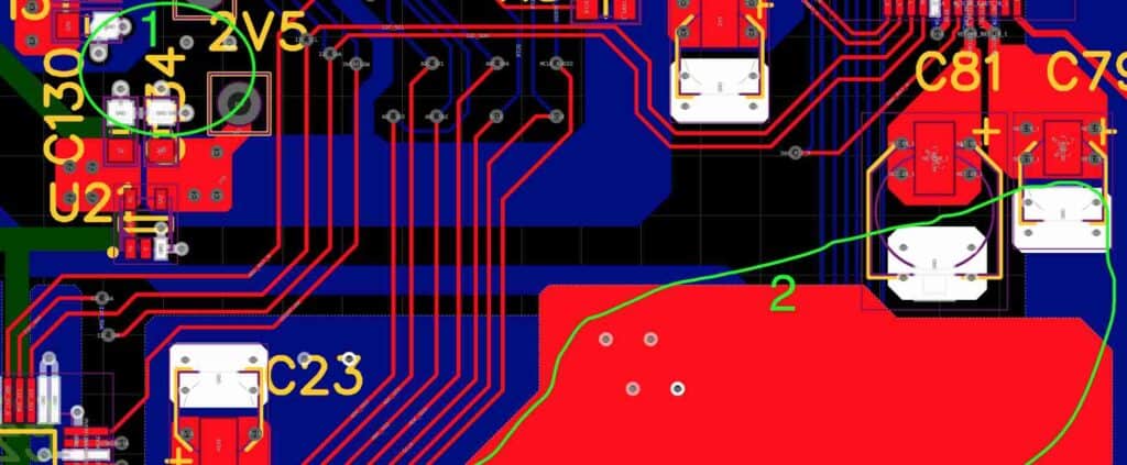
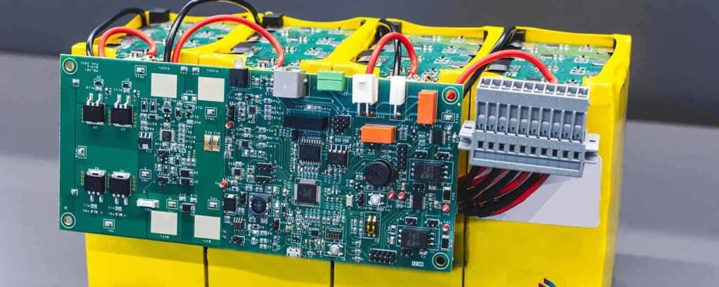
CB layout refers to the arrangement of components on a printed circuit board (PCB). It plays a crucial role in ensuring that the electronic device functions optimally. The layout of a PCB determines the performance, reliability, and cost of the device. A well-designed CB layout can reduce noise, improve signal integrity, and increase efficiency.
The CB layout process involves placing components, routing traces, and optimizing the design for manufacturability. The layout must consider factors such as power distribution, signal integrity, thermal management, and electromagnetic compatibility (EMC). A good CB layout should also be easy to assemble, test, and repair. In recent years, the demand for high-speed, high-density, and low-power devices has increased, making CB layout even more critical for electronic products.
What is CB Layout?
CB Layout is a type of printed circuit board (PCB) design that is used in the construction of electronic devices. It stands for “circuit board layout,” and is sometimes also referred to as “component layout” or “board layout.”
The purpose of a CB Layout is to lay out the various components of an electronic circuit in a way that is both functional and efficient. This involves arranging the components in such a way that they can be connected together by traces, or thin lines of conductive material, in order to create the desired circuit.
In order to create a CB Layout, a designer will typically start with a schematic diagram of the circuit, which shows the various components and how they are connected together. The designer will then use specialized software to lay out the components on the circuit board, taking into account factors such as the size and shape of the board, the placement of connectors and other external components, and the need to minimize interference between different parts of the circuit.
Overall, CB Layout is an important part of the process of designing and building electronic devices, and it requires careful planning and attention to detail in order to ensure that the resulting circuit is both functional and efficient.
Why is CB Layout Important?
CB Layout, or Circuit Board Layout, is a critical aspect of printed circuit board (PCB) design. It involves arranging the components and traces on a PCB to ensure that the circuit functions correctly and efficiently.
One of the primary reasons CB Layout is essential is that it can significantly impact the performance of the circuit. Poorly designed layouts can lead to interference, noise, and signal degradation, which can cause the circuit to malfunction or fail. A well-designed layout, on the other hand, can minimize these issues and ensure that the circuit operates as intended.
Another reason why CB Layout is crucial is that it can affect the cost and manufacturability of the circuit. A poorly designed layout may require additional components or a more complex manufacturing process, which can increase the cost of the circuit. A well-designed layout, on the other hand, can reduce the number of components and simplify the manufacturing process, resulting in a more cost-effective and manufacturable circuit.
Furthermore, CB Layout is essential for ensuring the safety and reliability of the circuit. A poorly designed layout can lead to short circuits, electrical leakage, and other safety hazards, which can be dangerous and even life-threatening. A well-designed layout can minimize these risks and ensure that the circuit is safe and reliable.
In summary, CB Layout is critical for ensuring the performance, cost-effectiveness, manufacturability, safety, and reliability of printed circuit boards. A well-designed layout can significantly improve the functionality and efficiency of the circuit while minimizing the risks and costs associated with poor design.
How to Create a CB Layout

Creating a CB layout can be a challenging task, but with the right tools and techniques, it can be done with ease. Here are some steps to follow when creating a CB layout:
-
Determine the board size: The first step in creating a CB layout is to determine the size of the board. This will depend on the number of components that need to be placed on the board and the size of the enclosure that will house the finished product.
-
Choose the right software: There are many software programs available for creating CB layouts. Choose one that is easy to use and has the features you need to create a professional-looking layout.
-
Place the components: Once you have chosen the software and determined the board size, it’s time to start placing the components on the board. Start with the larger components and work your way down to the smaller ones.
-
Route the traces: After placing the components, it’s time to route the traces. This is the process of connecting the components with copper traces on the board. Make sure to follow the manufacturer’s recommendations for trace width and spacing.
-
Check for errors: Before sending your design to production, make sure to check for errors. Use the software’s design rule check feature to ensure that there are no errors or design rule violations.
-
Send to production: Once your design is error-free, it’s time to send it to production. Choose a reputable manufacturer that can produce high-quality PCBs.
Creating a CB layout can be a challenging task, but by following these steps, you can create a professional-looking layout that meets your needs.
Tips for Optimizing CB Layouts
When it comes to designing a circuit board layout, there are several factors to consider to ensure optimal performance and reliability. Here are some tips to help you optimize your CB layouts:
1. Keep the Signal Path Short and Direct
The signal path is the path that the electrical signal travels from the source to the destination. To ensure the best signal integrity and minimize interference, it’s important to keep the signal path as short and direct as possible. Avoid routing signals around the board unnecessarily, and use vias and through-holes only when necessary.
2. Place Components Strategically
The placement of components on the board can have a significant impact on the performance of the circuit. Place components in a way that minimizes signal interference and maximizes thermal dissipation. Group components that generate heat together and place them near a heat sink or cooling fan.
3. Use Ground Planes
Ground planes are large areas of copper on the PCB that are connected to the ground. They help to reduce noise and provide a low-impedance return path for the signals. It’s important to ensure that the ground planes are uninterrupted and connected to all the ground pins of the components.
4. Follow Design Rules
Each PCB manufacturer has specific design rules that must be followed to ensure the board can be manufactured correctly. These include minimum trace widths, minimum clearance between traces, and minimum drill size. Make sure to follow these rules to avoid manufacturing issues and ensure the board works as intended.
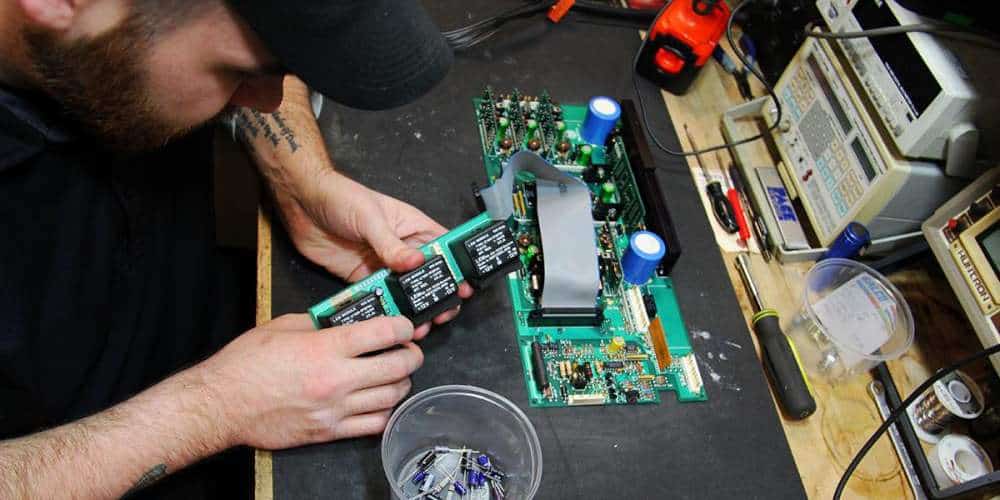
5. Test and Iterate
Testing is an essential part of the design process. Test the board thoroughly to ensure that it meets the design specifications and works as intended. If there are any issues, iterate on the design to fix them and test again.
By following these tips, you can optimize your CB layout and ensure that it performs reliably and meets the design specifications.
Common Mistakes to Avoid in CB Layouts
When designing a CB (circuit board) layout, there are several common mistakes that can lead to issues with the final product. Here are some of the most common mistakes to avoid:
1. Insufficient Trace Width
One of the most common mistakes in CB layout design is using insufficient trace width. This can lead to high resistance and voltage drops in the circuit, resulting in poor performance or even failure. It is important to ensure that the trace width is adequate for the current that will be flowing through it. A general rule of thumb is to use a trace width that is at least three times the size of the component lead that it is connected to.
2. Inadequate Ground Plane
Another common mistake is not providing an adequate ground plane. A ground plane is essential for reducing electromagnetic interference (EMI) and ensuring proper signal integrity. It is important to have a solid ground plane that covers the entire board, with no gaps or voids. Additionally, it is important to ensure that the ground plane is connected to all ground points on the board.
3. Poor Component Placement
Component placement is another critical aspect of CB layout design. Poor placement can lead to issues with signal integrity, EMI, and even thermal management. It is important to place components in a logical and efficient manner, with consideration given to signal flow, heat dissipation, and accessibility.
4. Inadequate Decoupling Capacitors
Decoupling capacitors are used to filter out noise and provide stable power to components. Inadequate decoupling can lead to issues with EMI, signal integrity, and even component failure. It is important to ensure that decoupling capacitors are placed close to the components they are filtering, and that their values are appropriate for the circuit.
5. Lack of Testing and Verification
Finally, one of the most common mistakes in CB layout design is not testing and verifying the design. It is important to perform thorough testing and verification of the design, including signal integrity testing, EMI testing, and functional testing. This can help to identify and correct any issues before the board is manufactured.
In conclusion, avoiding these common mistakes can help to ensure a successful CB layout design. By paying attention to trace width, ground planes, component placement, decoupling, and testing, designers can create high-quality, reliable circuits.
