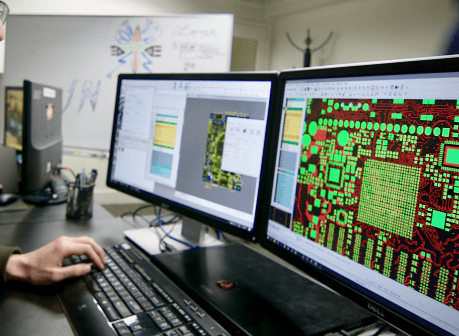
Designing your own printed circuit board (PCB) used to be a daunting task that required specialized knowledge and expensive software. However, with the advent of online PCB design tools, creating a custom PCB has become more accessible than ever before. These online tools allow you to design, prototype, and manufacture your own PCBs from the comfort of your own home or office.
One of the biggest advantages of using online PCB design tools is the ability to quickly iterate and modify your design. With traditional PCB design software, making changes to your design could be time-consuming and expensive. However, with online tools, you can easily make changes and see the results in real-time, allowing you to refine your design until it meets your exact specifications.
Another advantage of online PCB design tools is the ability to collaborate with others on your design. By sharing your design files with colleagues or friends, you can get feedback and suggestions on how to improve your design. This can be especially useful for those who are new to PCB design and may not have a lot of experience with the process.
Benefits of Designing Your Own PCB Online
Designing your own printed circuit board (PCB) online can be an excellent choice for both hobbyists and professionals. Here are some of the benefits of designing your own PCB online:
Cost Savings
Designing your own PCB online can save you a significant amount of money. Traditional PCB design methods require expensive software, hardware, and a lot of time to learn. With online PCB design tools, you can create a PCB design quickly and easily without the need for expensive equipment or software. Additionally, many online PCB design tools offer free or low-cost options, making it an affordable option for hobbyists.
Customization
When you design your own PCB online, you have complete control over the design process. You can customize the PCB to meet your specific needs, including the size, shape, and components used. This level of customization is not possible with pre-made PCBs. With online PCB design tools, you can easily make changes to the design as needed, and you can even order a prototype of your design to test it before committing to a large-scale production run.
Time Efficiency
Designing your own PCB online can save you a lot of time. Traditional PCB design methods can be time-consuming, requiring hours of work to create a single design. With online PCB design tools, you can create a design in a fraction of the time. Additionally, many online PCB design tools offer features such as auto-routing and design rule checking, which can further speed up the design process.
Overall, designing your own PCB online can be a cost-effective, customizable, and time-efficient option for both hobbyists and professionals. With the right online PCB design tool, you can create a high-quality PCB design quickly and easily.
How to Design Your Own PCB Online
Choose a PCB Design Tool
When it comes to designing your own PCB online, the first step is to choose a PCB design tool. There are many options available, both free and paid. Some popular choices include EasyEDA, Altium Designer, and Eagle PCB.
It’s important to choose a tool that fits your needs and skill level. If you’re just starting out, a simpler tool like EasyEDA might be a good choice. If you’re more experienced, you might prefer a more advanced tool like Altium Designer.
Create a Schematic
Once you’ve chosen a PCB design tool, the next step is to create a schematic. This is a diagram that shows the components and connections of your circuit.
When creating your schematic, it’s important to double-check that all components are properly connected and that there are no errors. This will save you time and money in the long run.
Design the PCB Layout
After creating your schematic, the next step is to design the PCB layout. This involves placing the components on the board and routing the connections between them.
When designing the PCB layout, it’s important to consider factors like component placement, trace width, and spacing. These factors can affect the performance and reliability of your circuit.
Generate Gerber Files
Once you’ve designed your PCB layout, the final step is to generate Gerber files. These are the files that are used to manufacture your PCB.
When generating Gerber files, it’s important to double-check that all layers and components are properly defined. This will ensure that your PCB is manufactured correctly.
In conclusion, designing your own PCB online can be a fun and rewarding experience. By following these steps and using the right tools, you can create a high-quality PCB that meets your specific needs.
Considerations When Designing Your Own PCB Online

When designing your own PCB online, there are several factors to consider. Here are some of the most important considerations to keep in mind:
PCB Size and Shape
Before designing your PCB, it’s essential to determine the size and shape of your board. The size and shape of your PCB will depend on the specific needs of your project. You should consider the available space for your PCB and its intended use. Make sure that your PCB’s size and shape will fit the enclosure or device you plan to use it in.
Number of Layers
The number of layers in your PCB will depend on the complexity of your circuit. The more complex your circuit, the more layers you will need. However, more layers also mean higher costs. Therefore, you should consider the trade-off between the complexity of your circuit and the number of layers required.
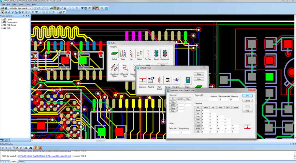
Trace Width and Spacing
The trace width and spacing are crucial factors in PCB design. The trace width determines the amount of current that can flow through a trace, while the spacing determines the distance between two traces. You should ensure that the trace width and spacing meet the requirements of your circuit design. You can refer to the manufacturer’s datasheet or use online calculators to determine the appropriate trace width and spacing.
Component Placement
The placement of components on your PCB is critical to the success of your project. You should ensure that the components are placed in a way that allows for efficient routing of traces. You should also consider the heat dissipation of your components and ensure that they are placed in a way that allows for adequate cooling.
Circuit Complexity
The complexity of your circuit will determine the difficulty of designing your PCB. You should consider the number of components, the number of connections, and the overall complexity of your circuit. You should also consider the experience level of the designer and the tools available for designing the PCB.
In conclusion, designing your own PCB online requires careful consideration of several factors. By considering the size and shape of your PCB, the number of layers, the trace width and spacing, component placement, and circuit complexity, you can ensure that your PCB is designed correctly and functions as intended.
Tips for Designing Your Own PCB Online

Double-Check Your Design
Before submitting your design for manufacturing, it’s crucial to double-check it for errors. Simple mistakes can cause significant issues and waste both time and money. Here are a few things to keep in mind when double-checking your design:
- Check for short circuits, open circuits, and other design errors.
- Verify that all components are correctly placed and oriented.
- Make sure that all of the necessary design files are included.
Use Design Rules
Design rules are essential to ensure that your PCB is manufactured correctly. They help to prevent errors and ensure that your design meets the manufacturer’s requirements. Here are a few design rules to consider:
- Minimum trace width and spacing
- Minimum drill size and annular ring
- Copper pour clearance
- Via pad size and spacing
When using design rules, it’s essential to make sure that they are consistent throughout your design.
Optimize Your Design for Manufacturing
Optimizing your design for manufacturing can help to reduce costs and improve the quality of your PCB. Here are a few things to keep in mind:
- Minimize the number of layers to reduce costs.
- Use standard components to ensure availability and reduce costs.
- Avoid placing components too close to the edge of the board.
- Use a consistent trace width and spacing to reduce manufacturing time.
By following these tips, you can ensure that your PCB design is error-free, meets the manufacturer’s requirements, and is optimized for manufacturing.
