It is a popular assumption that buying PCBs from online platforms is only possible for low-tech, small-batch prototypes. You can customize your circuit boards’ impedance control, layer count, and more with our help. We can manufacture boards with as many as sixteen layers, buried and blind vias, high-temp elements, and regulated impedance.
Knowing the location and method of fabrication of your circuitry is becoming important. Because the majority of PCB manufacturers adopt an online business model, there are some higher-tech circuits that a PCB firm may not be capable of producing. This is due to the unavailability of the proper machinery. The element of danger is also considerable.
Will you be purchasing a sixteen-layer PCB from an Asian company’s online store? Perhaps not, but it does occur. There are people that have no problem getting three PCBs for thirty-three dollars. It is inexpensive. But, when you consider the issues of quality and dependability. It’s not always the greatest option. The ideal way to order high-tech boards online is also questionable.
In this article, we’ll go over the steps you should take and avoid taking to ensure a seamless delivery of your online-purchased PCB to your dock.
The Online PCB Design software Purchasing
First, and most importantly, my suggestion is not to delay despite the fact that many of our clients use our web-based PCB ordering process. All of us have heard horror tales about organizing shipping by now. But, when Epec handles the cargo, we minimize the possibility of delays and act to fix any that do occur. It can be difficult to order PCBs online and have them shipped in a small box. Especially considering the current state of cargo both internationally and nationally. Our duration is of importance, and any further delays could have serious consequences.
Never fear using online buying and bidding for high-tech printed boards again with InstantPCBQuoteTM. Every case passes through a comprehensive DFM evaluation. So, before production, there will be no problems. Epec’s online PCB toolset makes it easy to order and get a twelve-layer PCB without buried/blind vias. We’ll get into some of the things that can go wrong when the layer count goes up later in the post.
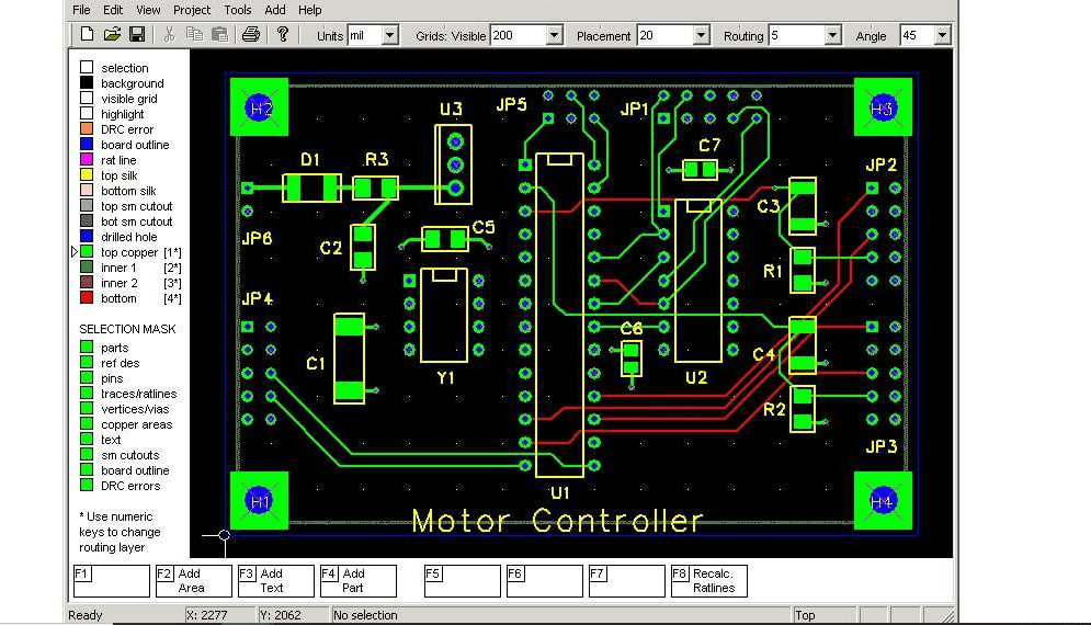
PCB Fabrication, Panel Layouts, Data Set, and Details
How can you ensure smooth delivery of your web-based PCB bid? Years of research have shown us that there’s a significant gap between the two types of data. Our clients range from OEMs to CMs to boutique engineering firms. The design deals they order from us might vary widely. In order to get your order processed quickly, manufactured accurately, and shipped to you on schedule, you need high-quality data collection.
On a monthly basis, we encounter a large number of data sets during the exact quotation, order, and engineering processes. We guarantee thorough and correct data sets and provide a free DFM solution to help our clients with machinability. Print all ground planes and circuits on all copper layers in either a negative or positive orientation. RS274X is the recommended format for the data. Most CAD programs support the RS274X file format, which makes it simple to import all the files including Gerber file without the need for additional manual work, such as the entry of apertures.
Printed Circuit Board Online Process

Always provide a one-to-one scale outline of the PCB profile for ease of production. The single board layout has usage in production for data setup, route programs, drilling, and scoring information.
1. Hole Dimensions
In an Excellon-format drill program, specify the tool dimensions that will produce the required hole dimensions. The production team will determine the proper drill diameter to achieve the final required hole size. If at all feasible, please include a drill table detailing the intended hole size, whether the hole has been drilled through or not, the desired amount of each bore type, and the allowable tolerance. The typical production tolerance for coated holes is +\-0.003 inch, whereas those for non-plated ones are +\-0.002 inch.
2. Soldering Mask
Please remember to add a solder mask on both sides, specify the color you’d want, and be aware that green is currently the most common color in the market. A wide range of hues get created; however, not every manufacturer can supply every flavor. Note where specific scaling is necessary for solder mask files; this will be possible at the production plant.
Please be aware that problems may arise on copper-to-copper separation of fewer than 0.009 inches when treating color schemes other than green. Solder masking can be badly affected by changes in pigment and chemistry used in the final finish. Thus this is still another thing that must get done before production can begin.
3. Silkscreen
Please only specify color when ordering silk-screened labels for one or perhaps both faces. The minimal width for printable, visible typeface is 0.005 inches, while the minimum height is 0.035 inches. In general, ordinary processing may not be able to replicate sizes less than this. CAD programs do not allow for resizing; all we can do is clip and relocate the text.
4. Fabrication Drawing
Information like board dimensions and tolerances should get included in the production drawing. Notes on the finished hole size, tolerance, and plating through/not plating through status, as well as whether or not the holes are plated through, should get recorded on the chart. You can get the details regarding the only PCB in a decent set of manufacturing notes. It’s fine if the manufacturing single PCB qty you receive are missing some details. We must know specifics, such as the total metal weight of the outer layers and the weight of the copper used in the inside layers. An accurate description of the weight would include the status of the copper finishing touches.
It is helpful to make a note of the RoHS, standard, and class when pricing a PCB so that the process of moving into production goes as smoothly as possible. Printed circuit boards are typically made in Class II or III facilities. Class III needs specialized handling at an increased expense and comprehensive paperwork in addition to Class II’s basic processing. If you need Class III PCBs, make sure your provider can make them.
5. Assessing If Your PCB Is Considered a High-Technology Circuit Board
High-tech PCBs are notoriously difficult to define. How can you determine whether you’ve upgraded a regular PCB with all the necessary features? It’s a large list, but it includes things like via-in-pad technique, buried or blind vias, 8 to 16 layers, tiny line widths of 0.005 inch or less, hole sizes of 0.008 inch or less, copper weights of 4 ounces or more, and PCB thicknesses of 0.125 inch or more.
For example, if the design of a four-layer PCB requires narrower trace and gap widths than the target metal weight allows for, then the design can be an advanced technology. For instance, a 1/2-ounce copper weight can be simply processed with a 0.005-inch trace and 0.005-inch gap. When the amount of copper used in a trace gets increased to 1 ounce, the processing and spacing requirements change. As the copper thickness doubles, it becomes considerably more challenging to recreate the finer trace and gap widths. When working with materials that have a greater copper weight, it is essential to leave more room for maneuver during processing in areas with tighter space and trace.
PCBs with six to sixteen layers are high-layer counts and high technology. The greater the number of layers, the more complicated the production process might become. A large percentage of layers with greater numbers will have buried and/or blind vias. Further complicating the order are instances where different sets of data of these whole kinds are present. The layer stack in which each set of interconnects resides should treat separately. How many times a part gets drilled, edge plating, and laminated affects how many sets of vias there are from the entry layer to the existing layer. There is a higher chance of junk and longer shipping cycles when buried, and blind vias get included in order. It takes a lot of time and money to complete each lamination cycle.
The castellated holes are another variant of the hole theme. The PCB has a hole drilled halfway through it, halfway off the edge. This hole should get bored into the PCB along the route process edge’s X and Y coordinates. For the plating barrel to remain flush with the hole edges, the holes must get drilled and plated first and then routed with specific processing. To assemble components at the end of the procedure, castellation is essential. Though some lifting, burring, or curling is expectable, given the difficulty of the procedure, it is minimizable with careful handling.
Prolonged processing times can also occur by PCBs with an excessively high overall thickness or a unique stack-up. Certain dielectrics restrict material processing control. There may be problems with delivery because there isn’t enough stock or because there isn’t enough of the necessary dielectric. The availability of specific sheet metal and copper weights varies. There is often a required minimum purchase size for those that have a premium price tag. While online ordering has made it easier to buy in smaller quantities, it has also made it more difficult to source materials with the required dielectric properties from a provider.
During assembly, PCBs have a layer called a solder mask put to them to shield the metal surface from shorting and oxidation. Applying a mask covering will make assembling much simpler. In most cases, a distance of 0.009 inches from metal to metal is ideal for mask adhesion to the lamination surface and for relief from inner copper surfaces. The processing difficulty increases below 0.009″, with 0.008″.
Conclusion
It is important to keep in mind that not all PCBs are manufacturable with the same fabrication resources. Therefore, not all PCBs online are fully functional. Though each printed circuit board is custom-made, the techniques involved in making them are quite similar. The features of the part are what make it difficult to manufacture. And not all production resources have the cutting-edge machinery or expertise to produce all varieties.
