Have you ever gone to a car dealership to buy a vehicle but you weren’t allowed to have a test-drive? Have you also tried to purchase a product online and only dissuaded because there is no “money back guarantee?”
We can go on and on with lots of examples, but the point is that the decision to buy a product or use a service is often influenced by what you expect to get out of it. The same applies to the electronics products, especially the Printed Circuit Boards (PCBs). If there is no means of validating the project, it only makes you skeptical.
It is for that reason that the Design Rule Check (DRC) was developed to help match the earliest designs with the outcome of a circuit board design. In this article, we talk about what a DRC PCB means and why it is relevant.
The Meaning of DRC PCB
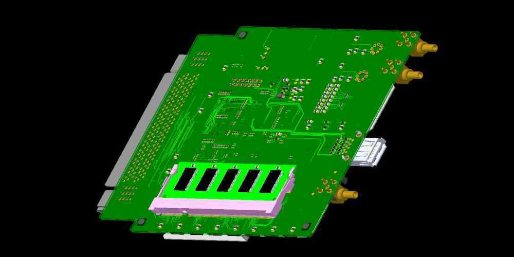
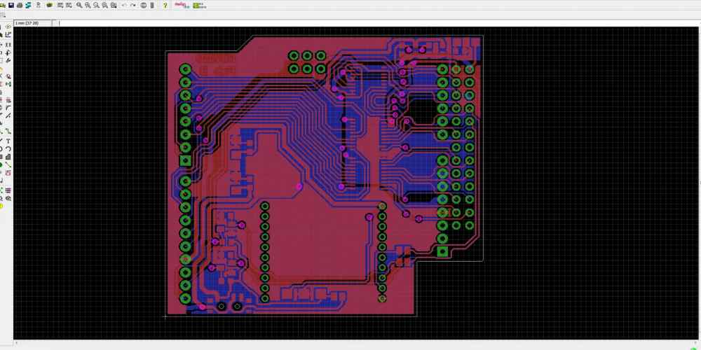
It means Design Rule Check (DRC). It is a process and set of rules used by the circuit board designer to not only match the design expectations with the outcome, but to also inspect the PCB for possible errors.
The importance of the DRC process is triggered by the fact that the circuit board design process is often prone to mistakes, which could be either from the designer or schematic’s perspective.
By using these rules, the designer has a better view of the components that are not well-placed, the mismatches in the trace widths and spacing, as well as other minor errors that might come up.
The List of Design Rule Checks for PCBs
Now that we are clear about what the DRC PCB means, let us look at some of the applicable rules.
DDR Fly-by Topology Rule
This is commonly used for the DDR designs that use the “fly-by topology rule.” The two core considerations here are the following:
- Confirming that the nets made with the fly-by topology are designed with the proper constraints.
- Ensuring that the accurate stub length is important.
Return Path Rule
This Design Rule Check (DRC) for PCBs has become a necessity, given the reduction in the sizes of modern circuit boards, as well as the increased requirements for high-speed circuit designs.
The “Return Path Rule” has to do with the confirmation that the PCB follows the ideal path rules. It also underscores the testing of the signals to confirm that they have a low-impedance return path.
Decoupling Capacitors’ Placement

One factor that could make all the difference in a PCB is how the components are placed. The decoupling capacitors, being one of the most important components, need to be placed accurately.
Using the Design Rule Check (DRC), the circuit board is automatically scanned to validate the accurate placement of the decoupling capacitors on each net.
If these capacitors are not positioned properly, the DRC PCB identifies the following:
- The non-existence of the capacitors and the;
- Improper placement of the decoupling capacitors.
Crosstalk Coupling Rule
This is one of the DRCs that must be followed to the latter. Crosstalk is one problem that could negatively affect how the signals are transmitted in the PCB.
The Crosstalk Coupling Rule has to do with the identification of the areas or locations where unwanted crosstalks occurred in the board. This is especially so for the sensitive nets.
DRC for Filer Placement
PCBs are susceptible to making noises. However, these noises are often suppressed or kept at the barest minimum via the use of filers. These filers are usually placed closer to the connector pins.
Therefore, the absence of the filers tends to cause the following issues:
- The suppression of the noises that might be present on the connector.
- Sensitive signals wouldn’t be protected when the filers are not in place.
- Also, it is possible for EMI issues to aggravate following the absence of filers close to the connector pins.
- Last but not least, the absence of filers tends to trigger radiation on the PCB.
The Rule for Checking the Ground and Power Widths
The widths of the power and ground planes are directly proportional to the performance of the board. If these widths are not positioned properly, it is possible for the DRC to pick these out.
What the Power and Ground Widths DRC looks out for are:
- The non-spaciousness of the ground traces.
- It also checks to see if the narrow trace has a narrow space.
If the above is tenable, it only means that there is not enough space for the current on the net to pass.
The aftermaths of this include unnecessary heat production and the insufficiency of power supply to the PCB components.
Using the Design Rule Check (DRC), we can also investigate the following in a PCB:
- Finding out if there has been a reduction in the outer rim of the power layer in a multilayered PCB. Confirming and fixing this on time helps to reduce the incidences of short-circuiting, especially when the power layer is exposed/open.
- The DRC PCB also checks if there are separate ground connections for the digital and analog circuits.
How to Implement DRC in PCBs
To do the Design Rule Check (DRC) in a circuit board, you need to use specific tools. The popular DRC tools are KiCAD EDA, Altium Designer and EasyEDA.
KiCAD’s advantage include providing readymade designs for PCBs, and making the process of running the DRC seamless. You can use it across different platforms, including Linux, macOS and Windows.
The benefit of using Altium Designer include the multiple circuit board design checking options and the 24/7 availability.
If you are looking for a DRC PCB tool that makes the entire process easier, it has to be EasyEDA. In living up to its name, the tool detects a wide range of errors, thereby, helping you to have lots of options to pick from.
Conclusion: DRC PCB vs. DFM & DFF
While Design Rule Check (DRC) is an excellent way to detect PCB errors, it has often been compared to other options.
On the one hand, it is compared to DFM and on the other, compared to DFF. The difference between the Design Rule Check (DRC) and the Design for Manufacturability (DFM) is that the former (DRC) has to do with detecting the design specifications that are out of or below the acceptable range, while the DFM has to do with the PCB design/layout topology that specifies how best to avoid the errors encountered in the board’s production.
The difference between the Design Rule Check (DRC) and the Design for Fabrication (DFF) because the former detects the issues/design errors, which if not checked, could negatively impact the PCB production process, which includes fabrication. The Design for Fabrication (DFF) process has to do with the detection and fixture of the issues arising from PCB fabrication.
To wrap it up, using the DRC PCB process is a sure way to detect design errors on time and have them fixed before shipping a circuit board.
