EasyEDA is a free, web-based software that enables users to design printed circuit boards (PCBs) with ease. The software is designed to be user-friendly, making it ideal for both beginners and experienced designers. With EasyEDA, designers can create schematics, PCB layouts, and even order PCBs directly from the software.
One of the standout features of EasyEDA is its extensive library of components. The library includes a wide range of commonly used components, such as resistors, capacitors, and transistors, as well as more specialized components. This library makes it easy for designers to find the components they need and quickly add them to their designs. Additionally, users can create their own custom components and add them to the library for future use.
Getting Started with EasyEDA
Creating a New Project
To get started with EasyEDA, you first need to create a new project. This can be done by clicking on the “New Project” button located at the top of the EasyEDA interface. You will then be prompted to enter a name for your project and choose a folder to save it in. Once you have done this, you can start designing your PCB.
Navigating the EasyEDA Interface
The EasyEDA interface is designed to be intuitive and user-friendly. The main window is divided into several sections, including the schematic editor, the PCB editor, and the library manager. You can switch between these sections by clicking on the corresponding tabs at the top of the window.
The toolbar at the top of the interface contains all the tools you need to create your PCB design. This includes tools for drawing schematics, placing components, and routing traces. You can also access various settings and options from the toolbar.
Adding Components to Your Design
To add components to your PCB design, you first need to open the library manager. This can be done by clicking on the “Library” button located in the toolbar. From here, you can browse through the available libraries and search for specific components.
Once you have found the component you want to use, you can simply drag and drop it onto the schematic editor. You can then connect the components together using the various tools and options available in the toolbar.
Overall, EasyEDA is a powerful and user-friendly tool for designing PCBs. With its intuitive interface and comprehensive set of features, it is an excellent choice for both beginners and experienced designers.
Designing Your PCB

Designing a PCB can be a daunting task, but with the right tools and knowledge, it can be straightforward and even enjoyable. EasyEDA is a free and user-friendly online PCB design tool that can help you create your PCB from start to finish. Here are the three main steps to designing your PCB with EasyEDA:
Schematic Capture
The first step in designing your PCB is to create a schematic. This is a graphical representation of your circuit that shows how all the components are connected. With EasyEDA, you can create your schematic by selecting the components you need from the built-in libraries and connecting them with wires. You can also customize your components or create your own libraries if needed. Once your schematic is complete, you can move on to the next step.
PCB Layout
The PCB layout is where you arrange the components on your board and create the physical design of your PCB. With EasyEDA, you can easily switch from the schematic view to the PCB layout view, where you can drag and drop your components onto your board and arrange them as needed. You can also add mounting holes, labels, and other design elements to make your PCB look professional and easy to use.
Routing Your PCB
Routing your PCB is the final step in the design process. This is where you create the traces that connect your components together and ensure that your circuit works as intended. With EasyEDA, you can use the built-in autorouter to automatically create your traces, or you can manually route your PCB to ensure complete control over the design. Once you have routed your PCB, you can generate your Gerber files and send them off to a PCB manufacturer to have your PCB fabricated.
In conclusion, designing a PCB with EasyEDA is a straightforward process that can be broken down into three main steps: schematic capture, PCB layout, and routing your PCB. With its user-friendly interface and powerful design tools, EasyEDA can help you create professional-looking PCBs that work as intended.
Design Verification and Exporting
Design Rules Checking
EasyEDA provides a Design Rules Checking (DRC) feature that allows you to verify your PCB design against a set of rules before exporting it. The DRC feature checks your design for errors such as overlapping traces, incorrect pad sizes, and clearance violations. You can customize the rules according to your requirements.
To run the DRC, click on the “Design Rules Check” button on the toolbar. EasyEDA will analyze your design and highlight any errors. You can then click on each error to see its details and fix it.
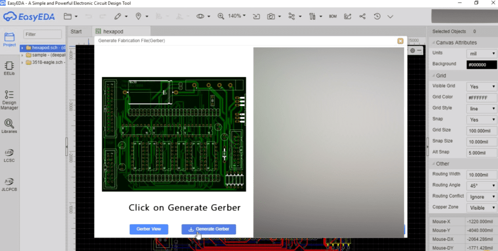
Gerber File Generation
Once you have verified your design, you can generate Gerber files for manufacturing. Gerber files are industry-standard files that contain the information required to manufacture your PCB. EasyEDA allows you to generate Gerber files for all the layers in your design, including the copper layers, solder mask layers, and silkscreen layers.
To generate Gerber files, click on the “Gerber” button on the toolbar. EasyEDA will generate a zip file containing all the Gerber files required for manufacturing.
Bill of Materials Export
EasyEDA also allows you to export a Bill of Materials (BOM) for your PCB design. A BOM is a list of all the components used in your design, along with their quantities and part numbers. The BOM makes it easy to order the components required for your PCB.
To export a BOM, click on the “BOM” button on the toolbar. EasyEDA will generate a CSV file containing the BOM information. You can then open the file in a spreadsheet program such as Excel and use it to order the components.
In conclusion, EasyEDA provides powerful design verification and exporting features that make it easy to verify your design and generate the files required for manufacturing. With these features, you can ensure that your PCB design is error-free and ready for production.
Collaborating and Sharing

Collaborating with Team Members
EasyEDA makes it easy to collaborate with team members on PCB designs. You can invite others to view or edit your design, and you can also assign roles to team members to control their level of access.
To collaborate with team members, simply click on the “Collaborate” button in the toolbar and enter the email addresses of the people you want to invite. You can also set their roles as “Viewer” or “Editor” depending on the level of access you want to grant them.
Once team members have access to the design, they can make changes and leave comments for others to review. EasyEDA automatically tracks all changes made to the design, so you can easily see who made what changes and when.
Sharing Your Design with Others
Sharing your PCB design with others is easy with EasyEDA. You can share your design as a URL or export it as a PDF, PNG, or SVG file.
To share your design as a URL, simply click on the “Share” button in the toolbar and copy the link. You can then send the link to others, and they can view your design in their web browser.
If you want to export your design as a file, simply click on the “Export” button in the toolbar and select the file format you want. You can then save the file to your computer and share it with others via email or file sharing services.
EasyEDA also allows you to embed your design in other websites or blogs using an iframe. This is a great way to showcase your design to a wider audience and get feedback from others.
Overall, collaborating and sharing with EasyEDA is simple and intuitive. Whether you’re working with a team or sharing your design with others, EasyEDA makes it easy to get your PCB design out there.
