Electronic Design Automation (EDA) is an essential aspect of modern electronics design. EDA refers to a set of software tools used by electronic engineers to design and analyze electronic systems. It is a vital tool for the development of advanced electronic devices, such as smartphones, laptops, and other electronic gadgets. EDA software enables engineers to design, simulate, verify, and test complex electronic systems before they are manufactured, thereby reducing the cost and time associated with product development.
EDA has revolutionized the electronics industry, making it possible to design and manufacture increasingly complex electronic systems. EDA tools enable engineers to design and simulate circuits, verify their functionality, and optimize their performance. They also provide tools for analyzing and improving system reliability, reducing power consumption, and minimizing electromagnetic interference. EDA tools have become an indispensable part of the electronics design process, and their importance is only expected to grow in the future. As electronic systems become more complex and the demand for faster and more efficient devices increases, EDA will continue to play a critical role in the development of advanced electronic systems.
Overview
What is EDA in Electronics?
EDA stands for Electronic Design Automation, which refers to a set of software tools used to design and analyze electronic systems. EDA tools help engineers to design, simulate, and verify complex electronic systems before they are manufactured. The EDA software includes tools for schematic capture, simulation, layout, and verification, among others.
Why is EDA important in Electronics?
EDA is essential in electronics because it helps to reduce design time, improve design quality, and reduce manufacturing costs. By using EDA tools, engineers can quickly evaluate different design options and optimize the design for performance, cost, and reliability. This results in faster time-to-market and lower development costs.
EDA tools also help to ensure that the design meets the required specifications and standards. This is critical in industries such as aerospace, automotive, and medical devices, where safety and reliability are paramount. EDA tools can simulate the behavior of the electronic system under different operating conditions and identify potential issues before the system is manufactured.
In summary, EDA is a critical part of the electronics design process, enabling engineers to design, simulate, and verify complex electronic systems quickly and accurately.
EDA Tools
In the field of electronics, Electronic Design Automation (EDA) tools play a vital role in the design and development of electronic circuits. These tools help engineers to design, analyze, and simulate electronic circuits more efficiently. There are different types of EDA tools available, such as simulation, layout, and verification tools.
Simulation Tools
Simulation tools are used to simulate the behavior of electronic circuits. These tools help engineers to analyze the performance of the circuit and identify any potential issues before the actual circuit is built. Some popular simulation tools include:
- SPICE (Simulation Program with Integrated Circuit Emphasis)
- LTspice
- Multisim
- PSpice
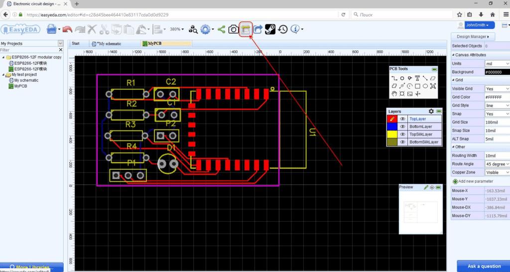
Layout Tools
Layout tools are used to create the physical layout of the electronic circuit. These tools help engineers to design the circuit board and place the components on it. Some popular layout tools include:
- Altium Designer
- Eagle PCB Design
- KiCAD
- OrCAD
Verification Tools
Verification tools are used to verify the correctness of the design. These tools help engineers to identify and correct any errors in the design before the circuit is built. Some popular verification tools include:
- Mentor Graphics ModelSim
- Synopsys VCS
- Cadence Incisive
- Aldec Active-HDL
In conclusion, EDA tools are essential for the design and development of electronic circuits. These tools help engineers to design, analyze, and simulate electronic circuits more efficiently. By using these tools, engineers can reduce the time and cost of the design process while improving the quality of the final product.
EDA Workflow

The Electronic Design Automation (EDA) workflow is a systematic approach to designing electronic systems. It involves a series of steps that include design entry, simulation and analysis, layout and verification, and design for manufacturability.
Design Entry
Design entry is the first step in the EDA workflow. It involves creating a schematic or a block diagram of the electronic system. This step is crucial as it sets the foundation for the rest of the design process. Design entry can be done using various software tools such as Cadence, Altium, or Eagle.
Simulation and Analysis
The next step in the EDA workflow is simulation and analysis. This step involves using simulation tools to test the design and analyze its performance. Simulation tools such as SPICE (Simulation Program with Integrated Circuit Emphasis) and Verilog are commonly used for this purpose. The simulation and analysis step helps identify design flaws and optimize the performance of the electronic system.
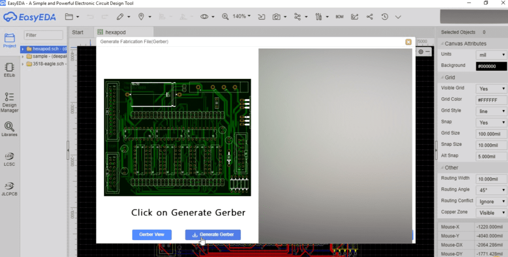
Layout and Verification
After simulation and analysis, the next step is layout and verification. This step involves creating a physical layout of the electronic system and verifying its functionality. The physical layout is created using software tools such as Cadence Virtuoso or Mentor Graphics. Verification tools such as Design Rule Checking (DRC) and Layout Versus Schematic (LVS) are used to ensure that the physical layout matches the original design.
Design for Manufacturability
The final step in the EDA workflow is design for manufacturability. This step involves optimizing the design for manufacturing. The goal is to ensure that the electronic system can be manufactured efficiently and cost-effectively. Design for manufacturability involves optimizing the layout, minimizing the number of layers, and reducing the complexity of the design.
In conclusion, the EDA workflow is a systematic approach to designing electronic systems. It involves a series of steps that include design entry, simulation and analysis, layout and verification, and design for manufacturability. Each step is crucial and helps ensure the success of the design process.
EDA Challenges

Complexity of Designs
One of the major challenges in EDA is dealing with the increasing complexity of electronic designs. As technology advances, the number of components on a circuit board increases, and the size of the board decreases. This makes it more challenging to design, test, and debug electronic systems. As a result, engineers need to use more advanced EDA tools to manage the complexity of designs.
Integration with Other Tools
Another challenge in EDA is the integration of EDA tools with other tools in the design flow. EDA tools need to work seamlessly with other design tools such as simulation, verification, and synthesis tools. This requires a high level of interoperability between different tools, which can be challenging to achieve. Engineers need to ensure that the tools they use are compatible with each other to avoid any issues in the design flow.
Cost and Time Constraints
The cost and time constraints associated with EDA are also significant challenges. EDA tools can be expensive, and the cost of maintaining and upgrading them can add up over time. Additionally, the time it takes to design, test, and verify a system can be significant, which can delay product development and time-to-market. Engineers need to balance the need for high-quality designs with the need to meet cost and time constraints.
In summary, EDA faces several challenges, including the increasing complexity of designs, the integration of EDA tools with other tools in the design flow, and cost and time constraints. Engineers need to use advanced EDA tools and ensure that they are compatible with other tools in the design flow to overcome these challenges.
