When it comes to printed circuit board (PCB) prototyping, there is a myriad of fascinating and crucial information to consider. As the foundation for countless electronic devices, PCBs play an indispensable role in modern life. Before diving deeper into the complexities of PCB prototyping, it’s crucial to understand 12 insane (but true) things that every enthusiast, engineer, or industry professional needs to know.
First, the rapid advancement of technology has led to impressive developments in PCB prototyping, making it easier and more affordable than ever. Innovations in software, manufacturing processes, and material science are transforming the industry at an unprecedented speed. This knowledge empowers professionals and hobbyists alike to produce intricate designs, even in small quantities.
Second, PCB prototyping is not a one-size-fits-all process; understanding the various methodologies available is essential for success. From DIY approaches to partnering with professional manufacturers, each approach has unique benefits and challenges. Selecting the right path for your project depends on multiple factors, including budget, design complexity, and desired turnaround time. With these factors in mind, one can make informed decisions when navigating the exciting world of PCB prototyping.

What Are PCB Prototypes
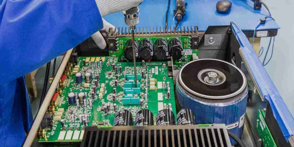
PCB prototypes are an essential part of the electronic product development process. They serve as proof-of-concept for your design and are used for testing and validation purposes before moving on to the production phase.
A PCB prototype is an early sample or proof-of-concept of the final PCB (Printed Circuit Board) that will be used in an electronic device. Designers create PCB prototypes to test and refine their circuit designs, ensuring that they work as intended, have the desired performance, and can be manufactured efficiently.
PCB design software allows designers to create digital representations of the circuit layout, placing components such as resistors, capacitors, and integrated circuits on the board. The designer also sets up the required electrical connections between the components by creating copper traces, which act as conductive pathways.
Once the digital design is complete, the prototype can be produced using a variety of methods, such as:
- Etching: A process that removes excess copper from the board, leaving only the desired traces.
- Lamination: The process of bonding multiple layers of PCB material together to create the desired board thickness and complexity.
- Photolithography: A technique using light-sensitive materials to create intricate patterns of traces and components.
PCB prototypes can be built in-house or outsourced to specialized manufacturers who can turn around a prototype in as little as 24 hours. Rapid prototyping reduces the risk of costly errors, allowing for quicker adjustments to the design and ultimately, a faster time-to-market.
Key benefits of PCB prototyping include:
- Early detection of design flaws and performance issues
- Enhanced testing and validation capabilities
- Reduced development costs and lead times
- Improved manufacturability and product quality
PCB prototypes are crucial for the success of any electronic product design, as they provide valuable insights into the performance and manufacturability of the final product, saving time, money, and ensuring a successful outcome.
Types of PCB Prototyping
When it comes to PCB prototyping, there are several methods used to bring a design to life. These can be categorized into three main approaches: Rapid Prototyping, Low Volume Production, and High Volume Production.
Rapid Prototyping
Rapid Prototyping is a process that quickly creates a functional version of a PCB design within a comparatively short timeframe. It’s an ideal method to:
- Validate and test designs before full-scale production
- Quickly iterate on design changes
- Reduce time to market for new products
Some key features of rapid prototyping include:
- Quick turnaround times, typically within 24-72 hours
- Use of specialized equipment and materials designed for speed
- May include 3D printing or CNC milling for creating board structures
Low Volume Production
Low Volume Production is a PCB prototyping method that addresses the needs of small-scale manufacturing. This may be used when a business:
- Requires a smaller number of units, typically under 1,000
- Prefers to run a pilot or test batch before large-scale production
- Produces specialized or niche products with limited demand
Some benefits of low volume production include:
- Lower initial investment costs
- Quicker turnaround than high volume production
- Higher level of flexibility for design changes
High Volume Production
High Volume Production refers to the full-scale manufacturing of PCBs in large quantities. This approach is typically employed when:
- Demand for the product is well-established
- Unit cost reduction is a priority
- Consistent quality and streamlined processes are crucial
High Volume Production provides these advantages:
- Economies of scale leading to lower unit costs
- Rigorous quality checks and streamlined processes
- Dedicated production lines for efficient manufacturing
Materials Used in PCB Prototypes

FR4
FR4 is one of the most widely used materials in PCB Prototypes due to its versatility and relatively low cost. FR4 is a composite material made up of woven fiberglass cloth and epoxy resin, which provides excellent electrical insulation properties. FR4 is known for its:
- High heat resistance
- Good mechanical strength
- Excellent chemical resistance
- High dimensional stability
Aluminum
Aluminum PCBs are another popular choice in the industry, offering unique benefits like better heat dissipation and durability. Some key advantages of using aluminum as a PCB material include:
- Excellent thermal conductivity
- Lightweight, yet sturdy construction
- Greater design flexibility
- Eco-friendly, recyclable material
Rogers Material
Rogers Material is a high-frequency laminate developed by Rogers Corporation. This material is ideal for applications with specific performance requirements or high-frequency applications. Rogers Material has several characteristics that make it a preferred choice:
- Low dielectric loss
- Low signal attenuation
- High thermal conductivity
- Stable performance across a wide range of temperatures
Each of these PCB materials offers distinct benefits, depending on the needs of your prototype project. It is essential to carefully evaluate your requirements and desired outcomes before choosing the right material for your application.
PCB Design Considerations
Layout Design
When designing a PCB layout, it’s crucial to consider the placement and routing of components. This ensures signal integrity, minimizes the risk of electromagnetic interference (EMI), and optimizes board space. Start by placing critical components such as power supply regulators, followed by analog components and then digital components. Keep high-speed signals short and provide sufficient distance between components to avoid thermal issues.
Copper trace width and thickness should be taken into account for current-carrying capacity and signal integrity. Incorporate ground and power planes to improve noise immunity and minimize voltage drops.
Solder Mask
The solder mask is a crucial element in the PCB manufacturing process. It serves as a protective layer, preventing oxidation and preserving the integrity of the copper traces underneath. It also provides mechanical support to avoid solder bridging, ensuring proper electrical connections between components and the PCB.
There are several solder mask types, each with its own advantages and disadvantages. Common types include:
- Liquid Photoimageable (LPI)
- Dry Film Photoimageable
- Thermal Curable
Choose the solder mask type based on your specific application requirements and budget. Regardless of the type used, it’s essential to follow the manufacturer’s guidelines for the solder mask thickness and application process to ensure optimal performance and reliability.
Fabrication Methods
There are several fabrication methods used to create PCB prototypes. In this section, we will discuss three popular methods: milling, chemical etching, and laser cutting.
Milling
Milling is a subtractive process that involves using a computer-controlled machine to carve out parts of a PCB from a solid board. This technique is effective for quick turnaround times and small-batch production.
- Suitable for prototypes and small batch production
- Minimal material waste
- Can create complex PCB designs
However, milling has some limitations, such as the inability to create very small traces and the challenge of achieving tight tolerances.
Chemical Etching
Chemical etching is a widely used fabrication method for PCBs. It involves using chemicals to remove excess material from the board, leaving only the desired circuit pattern. A resist, usually a photoresist, is applied to the board to protect the circuit pattern from the etching chemicals.
- Works well for medium to high volumes
- Can create fine traces and tight tolerances
There are some drawbacks, though. Handling hazardous chemicals and disposing of them properly requires strict safety protocols. In addition, the process can be time-consuming and may not be suitable for rapid prototyping.
Laser Cutting
Laser cutting is a non-contact technique that uses a high-powered laser beam to cut PCBs to the desired shape and size. This process is excellent for creating complex designs and intricate patterns.
- High precision and accuracy
- Ideal for complex designs
- No need for chemicals
Laser cutting can be expensive compared to other fabrication methods, especially for small-scale production. It also may not be suitable for materials that are heat-sensitive or materials with high reflectivity.
Assembly Techniques
Through-Hole Technology
Through-Hole Technology (THT) is a traditional method in PCB assembly where components are inserted through holes on the printed circuit board. THT has the following characteristics:
- Durability: Components mounted using THT are mechanically strong, making them suitable for high-stress situations.
- Manual Assembly: THT generally requires more manual labor for assembly compared to Surface Mount Technology.
- Ease of Repairs: THT components can be easily replaced or repaired since they are easier to reach and desolder.
Some common applications of THT include power supplies, automotive electronics, and industrial equipment.
Surface Mount Technology
Surface Mount Technology (SMT) involves mounting components directly onto the surface of PCBs. The key features of SMT include:
- Higher Component Density: SMT allows for more components to be placed on the board, resulting in higher component density.
- Automated Assembly: SMT is compatible with automated assembly processes, increasing efficiency and reducing labor costs.
- Miniaturization: The reduced size of SMT components enables the creation of smaller and lighter electronic devices.
| Advantages | Through-Hole Technology | Surface Mount Technology |
|---|---|---|
| Durability | Stronger connections | Weaker connections |
| Assembly | Manual, slow proces | Automated, faster process |
| Component Density | Lower | Higher |
| Size | Larger components | Smaller components |
SMT has become the industry standard for PCB assembly due to its increased efficiency, smaller component size, and higher component density. However, THT is still prevalent in specific applications that require more robust connections and easier repairability.
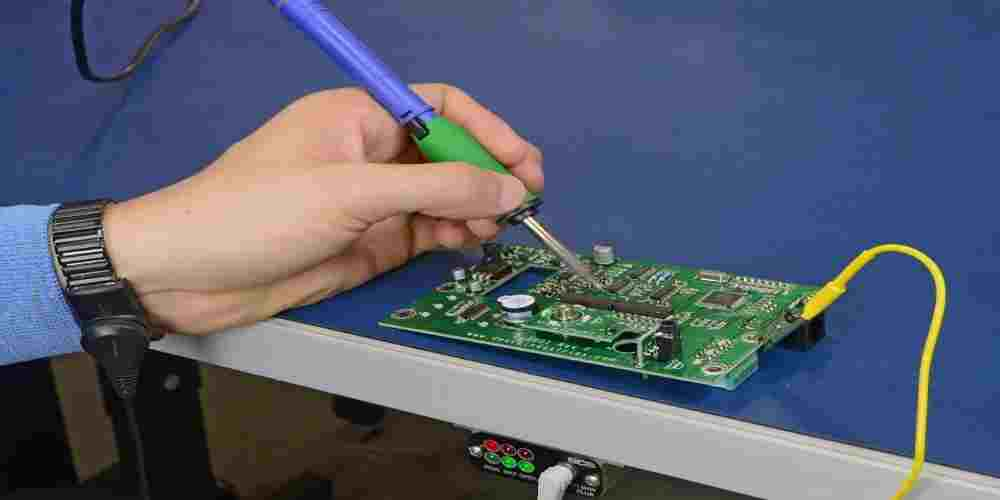
Quality Testing and Inspection
For PCB prototypes, quality testing and inspection are crucial to ensure the proper functioning of the final product. In this section, we will discuss two essential testing methods: Automated Optical Inspection (AOI) and X-Ray Inspection.
Automated Optical Inspection (AOI)
Automated Optical Inspection or AOI is a non-contact test method that uses an optical scanning system to inspect printed circuit boards (PCBs) for defects. Here are some key benefits and features:
- Rapid defect detection: AOI is capable of inspecting PCBs at a high speed, ensuring a faster production cycle.
- Accuracy: AOI systems can detect a wide range of defects, including missing or misplaced components, solder bridges, and copper overlaps.
- Cost-effective: As a non-contact method, AOI minimizes the risk of damage to the PCBs during the inspection process.
X-Ray Inspection
X-Ray inspection is another valuable method for assessing the quality of PCB prototypes, particularly for inspecting the solder joints of surface-mount technology components. Here are the main advantages:
- In-depth inspection: X-Ray inspection can reveal issues that are not visible to the naked eye or AOI. This includes voids, cracks, and insufficient solder joints.
- Non-destructive: Similar to AOI, X-Ray inspection is a non-contact method that reduces the risk of causing damage to the PCBs.
In summary, both AOI and X-Ray inspection are essential tools for ensuring the quality and reliability of PCB prototypes. By using these inspection methods, manufacturers can identify and rectify any defects before the final production, resulting in a higher-quality end product.
Cost Factors for PCB Prototyping
Board Complexity
The complexity of a PCB is one of the primary factors that influences prototyping costs. More complex boards require additional layers, vias, and traces, which in turn increases manufacturing and assembly costs. Generally, costs increase as the layer count, signal routing complexity, and component density increase. Some key aspects affecting complexity include:
- Number of layers
- Trace width and spacing
- Via types (through-hole, blind, buried)
- Component count and packaging
Material Choices
Another factor contributing to PCB prototyping costs is the choice of materials used in the fabrication process. The physical properties of these materials, such as thermal conductivity and dielectric constant, can impact the overall performance of the PCB. Material choices also influence the ease of manufacturing and final price. Some common PCB materials are:
- FR4: Standard, cost-effective choice for most applications
- High-Temperature (HT) FR4: Improved thermal performance at higher cost
- Rogers: Enhanced signal integrity but more expensive
In addition to the core materials, the selection of surface finishes and soldermask types can also affect the cost. Examples of surface finishes include:
- HASL (Hot Air Solder Leveling)
- ENIG (Electroless Nickel Immersion Gold)
- OSP (Organic Solderability Preservative)
Each of these finishes has its own cost implications, so it’s essential to choose the appropriate finish based on performance, reliability, and budget requirements. The same principle applies to soldermask, where standard and premium options can influence cost.
Consideration of both board complexity and material choices is essential for managing PCB prototyping costs, ensuring that the final product meets performance requirements, and adheres to budget constraints.
Timeline for PCB Prototyping
The process of PCB prototyping has evolved significantly over the years. Here is a brief timeline highlighting important milestones in PCB prototyping history:
-
1920s: The first patented PCBs were made using a phenolic insulating material with copper foil laminated on one side.
-
1930s-1940s: During World War II, the necessity for rapid prototyping of electrical circuits gave birth to the development of wire-wrap technology, where engineers could quickly create PCB prototypes by wrapping insulated wires together.
-
1950s: The invention of the photoengraving process revolutionized the PCB industry, as it allowed for more precise and consistent designs, enabling the mass production of PCB prototypes.
-
1960s-1970s: Multilayer PCBs were introduced, leading to reduced size and increased complexity of electronic devices. Around this time, Surface Mount Technology (SMT) also emerged, enabling the miniaturization of electronic components and making PCB prototyping more efficient.
| Decade | Key Milestone |
|---|---|
| 1920s | Invention of phenolic PCBs |
| 1930s-40s | Development of wire-wrap |
| 1950s | Photoengraving process |
| 1960s-70s | Multilayer PCBs and SMT |
Fast forward to today, and we have several advanced methods of creating PCB prototypes. Some recent advancements in the field include:
-
CAD software: Computer-Aided Design (CAD) software has become essential for designing complex circuits efficiently. This allows engineers to visualize the circuit before printing, minimizing errors and reducing the time spent troubleshooting.
-
3D printing: The use of 3D printers in the prototyping process has become more prevalent, enabling quicker turnaround times, lower costs, and increased prototype accuracy.
-
Flexible PCBs: The development of flexible materials for PCB prototyping has led to innovations in wearable technology and more compact, foldable electronics.
In conclusion, PCB prototyping has evolved greatly since its inception in the early 20th century. Advancements in materials, technology, and design methods have allowed the industry to create more complex, miniaturized prototypes at a faster rate and lower cost than ever before.
Common Challenges and Solutions
Tight Component Placement
In PCB prototyping, tight component placement might pose challenges in terms of routing and soldering. Designers need to be careful with:
- Traces: Ensure that traces have enough clearance between each other to prevent short circuits.
- Via size: Opt for smaller-sized vias to make space for other components.
- Component density: Balance the density of components to maintain the integrity of the signal.
Some solutions to address these challenges are:
- Utilize both sides of the PCB for components.
- Employ surface-mount technology (SMT) for a more compact design.
- Opt for high-density interconnect (HDI) technology to create more routing channels.
Thermal Management
Proper thermal management is crucial for the longevity and optimum performance of a PCB. Common challenges involve:
- Hotspots: Areas with high heat generation can potentially affect surrounding components.
- Insufficient heat dissipation: Poor thermal conductivity of PCB material may lead to overheating.
- Thermal expansion: Mismatched expansion rates between PCB layers can cause mechanical stress on components.
To counter these challenges, consider the following solutions:
- Plan a thermal management strategy early in the design process.
- Use thermal vias and copper planes to spread and dissipate the heat.
- Select high-quality PCB materials with appropriate thermal conductivity.
Environmental Considerations
RoHS Compliance
PCB prototypes need to follow RoHS (Restriction of Hazardous Substances) compliance to minimize the negative environmental impact. RoHS aims to restrict harmful components like lead, mercury, and cadmium in electronic products. It’s crucial to work with manufacturers who adhere to these guidelines when producing PCB prototypes.
- Lead-free soldering
- Proper labeling
By ensuring RoHS compliance, PCB prototypes contribute to reducing harmful substances and creating sustainable products.
Recycling
Recycling is an essential aspect to consider during PCB prototyping. The recycling process reduces electronic waste and helps save resources. To facilitate recycling:
- Use non-hazardous materials
- Focus on the design stage
Recycling PCB prototypes should involve the recovery of precious metals like gold, silver, and copper for reuse in new products.
In summary, environmental considerations such as RoHS compliance and recycling are critical aspects of PCB prototyping that help promote a greener and sustainable electronics industry.
