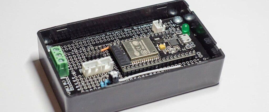
ESP 01 is a popular WiFi module that is widely used in the Internet of Things (IoT) projects. It is a small and low-cost device that can connect to a WiFi network and communicate with other devices over the internet. The ESP 01 module is based on the ESP8266 chip, which is a powerful and versatile microcontroller that can be programmed using the Arduino IDE.
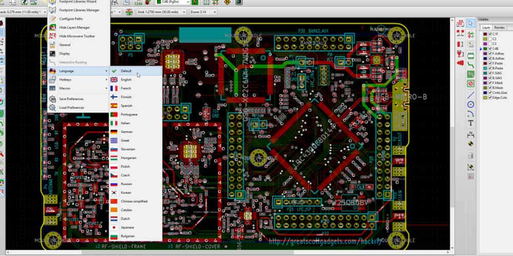
One of the most important aspects of using the ESP 01 module is designing the PCB layout. The PCB layout is the physical design of the printed circuit board that connects the ESP 01 module to other components and devices. A well-designed PCB layout can ensure the proper functioning of the ESP 01 module and prevent issues such as interference, noise, and signal loss. In this article, we will discuss the best practices for designing an effective PCB layout for the ESP 01 module. We will cover topics such as component placement, trace routing, ground planes, and signal integrity. By following these guidelines, you can create a reliable and efficient PCB layout for your ESP 01 project.
Overview of ESP 01 PCB Layout
What is ESP 01 PCB Layout?
ESP 01 PCB Layout is a printed circuit board (PCB) design specifically for the ESP8266 Wi-Fi module, also known as the ESP-01. The ESP-01 is a popular and cost-effective module for adding Wi-Fi connectivity to projects, and the PCB layout is designed to make it easier to use in your designs. The layout includes all the necessary components for the module, such as voltage regulators, capacitors, and resistors, as well as headers for connecting to other devices.
Why is ESP 01 PCB Layout Important?
Using the ESP 01 PCB Layout can save you time and effort in designing your own PCB for the ESP-01 module. The layout has already been tested and optimized for the module, so you can be sure that it will work correctly. It also provides a more compact and organized solution than using a breadboard or wiring the module directly to your project. Additionally, the layout includes all the necessary components for the module, which can help ensure stable and reliable performance.
In summary, ESP 01 PCB Layout is a convenient and efficient way to incorporate the ESP-01 Wi-Fi module into your projects. By using the pre-designed layout, you can save time and effort while also ensuring reliable performance.
Design Considerations for ESP 01 PCB Layout
When designing a printed circuit board (PCB) for the ESP 01 module, there are several important design considerations to keep in mind. These considerations can help ensure that the PCB functions properly and reliably.
Power Supply Considerations
The ESP 01 module requires a stable power supply to function properly. When designing the PCB, it is important to ensure that the power supply meets the following requirements:
- Voltage: The ESP 01 module requires a voltage of 3.3V. The power supply should be designed to provide a stable 3.3V output.
- Current: The ESP 01 module can draw up to 250mA of current during transmission. The power supply should be designed to provide sufficient current to meet this requirement.
- Noise: The power supply should be designed to minimize noise and ripple. This can be achieved by using a low-dropout (LDO) voltage regulator and adding bypass capacitors.
Signal Integrity Considerations
Signal integrity is critical to the proper functioning of the ESP 01 module. When designing the PCB, it is important to ensure that the following signal integrity considerations are taken into account:
- Grounding: The ESP 01 module should be properly grounded to minimize noise and interference.
- Trace Length: The length of the traces should be kept as short as possible to minimize signal loss and interference.
- Impedance Matching: The impedance of the traces should be matched to the impedance of the ESP 01 module to minimize reflections and signal loss.
Layout Considerations
The layout of the PCB can also have a significant impact on the performance of the ESP 01 module. When designing the PCB, it is important to consider the following layout considerations:
- Antenna Placement: The antenna should be placed as far away from other components as possible to minimize interference.
- Component Placement: The components should be placed in a logical and organized manner to minimize signal interference and crosstalk.
- Ground Plane: A ground plane should be used to provide a low-impedance return path for the signals and to minimize interference.
By taking these design considerations into account, it is possible to design a PCB that functions properly and reliably with the ESP 01 module.
ESP 01 PCB Layout Best Practices

Component Placement
Proper component placement is crucial for the functionality of the ESP 01 PCB layout. Here are some best practices to follow:
- Place components in a logical and organized manner to minimize signal interference and noise.
- Place decoupling capacitors close to the power pins of the components they are protecting.
- Place the ESP 01 module away from high-frequency components to prevent interference.
- Place connectors and switches on the edges of the board for easy access.
Routing Guidelines
Routing is the process of connecting the components on the PCB. Here are some routing guidelines to follow:
- Keep traces as short as possible to minimize signal delay and noise.
- Use wider traces for high-current components to prevent overheating.
- Route sensitive signals away from noisy areas of the board.
- Avoid crossing traces to prevent signal interference.
Grounding Techniques
Grounding is essential for the proper functioning of the PCB. Here are some grounding techniques to follow:
- Use a ground plane to provide a low-impedance path for the return current.
- Connect all ground pins of the components to the ground plane.
- Use multiple vias to connect the ground plane to the bottom layer of the board.
- Keep the ground plane away from high-frequency components to prevent interference.
Following these best practices will ensure a functional and reliable ESP 01 PCB layout.
Tools and Resources for ESP 01 PCB Layout
Schematic Capture Tools
When designing a PCB layout for the ESP 01 module, it is essential to have a good schematic capture tool. Some popular options include Eagle PCB, KiCAD, and Altium Designer. These tools allow you to create a schematic diagram of your circuit, which you can then use to generate a PCB layout.
PCB Layout Tools
After creating a schematic diagram, you need to create a PCB layout. Some popular PCB layout tools include Eagle PCB, KiCAD, Altium Designer, and DipTrace. These tools allow you to place components and traces on a board, and then generate Gerber files that can be sent to a manufacturer for fabrication.
Reference Designs and Datasheets
When designing a PCB layout for the ESP 01 module, it is helpful to have reference designs and datasheets available. The ESP 01 datasheet provides information on the pinout, electrical characteristics, and programming interface of the module. Additionally, there are many reference designs available online that can be used as a starting point for your own design.
It is important to note that while reference designs can be helpful, they should not be copied directly. Instead, they should be used as a starting point for your own design, and modified to meet your specific requirements.
In conclusion, when designing a PCB layout for the ESP 01 module, it is important to have access to good schematic capture and PCB layout tools, as well as reference designs and datasheets. By using these tools and resources, you can create a high-quality PCB layout that meets your specific requirements.
