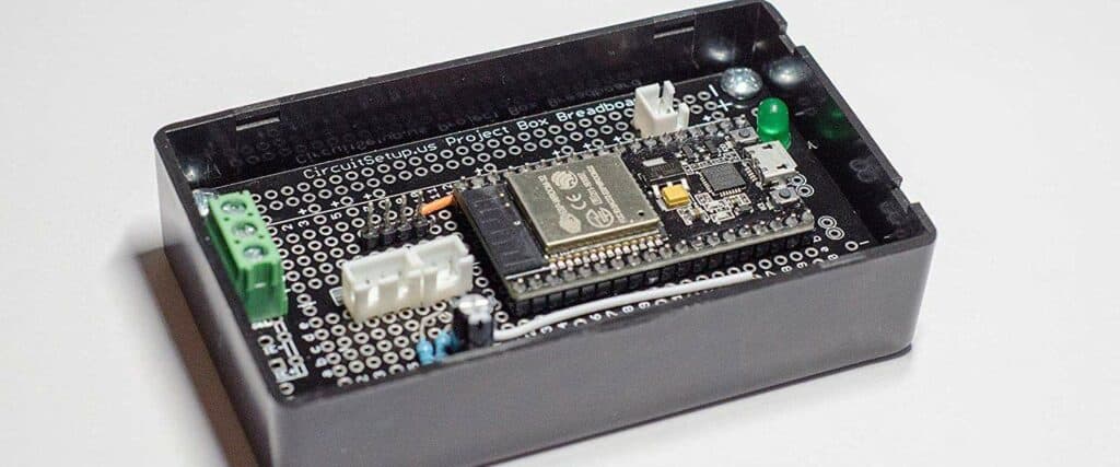
ESP8266 12E is a popular Wi-Fi module that is widely used in IoT projects. The module’s small size, low power consumption, and low cost make it a popular choice for DIY enthusiasts and professionals alike. However, designing a printed circuit board (PCB) layout for the ESP8266 12E module can be a challenging task, especially for beginners. In this article, we will discuss some tips and tricks for designing an efficient and reliable PCB layout for the ESP8266 12E module.
The ESP8266 12E module has a compact form factor and a complex pin layout, which can make it difficult to design a PCB layout that meets all the requirements. One of the most important considerations when designing a PCB layout for the ESP8266 12E module is to ensure that the power supply and signal traces are properly routed to avoid interference and noise. Additionally, the module requires a stable and clean power supply, which can be achieved by using a dedicated voltage regulator and filtering capacitors.
Another important aspect of designing a PCB layout for the ESP8266 12E module is to ensure that the module is properly grounded. Grounding is critical to prevent noise and interference from affecting the module’s performance. It is also important to ensure that the PCB layout is optimized for the specific application and environment in which the module will be used. By following these guidelines, designers can create a reliable and efficient PCB layout for the ESP8266 12E module.
PCB Design Considerations
When designing a PCB layout for an ESP8266-12E module, there are several important considerations to keep in mind. These considerations include schematic design, component placement, and trace routing.
Schematic Design
The first step in designing a PCB layout for an ESP8266-12E module is to create a schematic. The schematic should include all of the necessary components for the module to function properly, including the ESP8266-12E module itself, as well as any additional components such as voltage regulators, capacitors, and resistors.
Component Placement
Once the schematic has been designed, the next step is to place the components on the PCB. When placing components, it is important to consider the size of the PCB, as well as the size of the components themselves. It is also important to ensure that components are placed in a way that allows for easy access and maintenance.
Trace Routing
The final step in designing a PCB layout for an ESP8266-12E module is to route the traces. When routing traces, it is important to consider the length of the traces, as well as the width of the traces. It is also important to ensure that the traces are routed in a way that minimizes noise and interference.
In conclusion, designing a PCB layout for an ESP8266-12E module requires careful consideration of schematic design, component placement, and trace routing. By following these considerations, it is possible to create a PCB layout that is both functional and easy to maintain.
Power Supply

Voltage Regulator Selection
Choosing the right voltage regulator is crucial for the ESP8266 12E PCB layout. The voltage regulator should be able to handle the input voltage and output voltage required by the ESP8266 module. The most commonly used voltage regulator is the LM7805, which can handle an input voltage of up to 35V and output a constant 5V. However, it is recommended to use a switching regulator as it is more efficient and generates less heat.
Capacitor Selection
Capacitors are essential components in the power supply circuit as they help stabilize the voltage and filter out noise. Two capacitors are required in the power supply circuit, a ceramic capacitor and an electrolytic capacitor. The ceramic capacitor should be placed as close as possible to the voltage regulator’s input pin to reduce noise. The electrolytic capacitor should be placed as close as possible to the voltage regulator’s output pin to stabilize the voltage.
When selecting capacitors, it is important to choose capacitors with the correct capacitance and voltage rating. The voltage rating should be higher than the input voltage, and the capacitance should be chosen based on the current requirements of the circuit.
In summary, choosing the right voltage regulator and capacitors is crucial for a stable and efficient power supply for the ESP8266 12E PCB layout.
Antenna Design
Antenna Selection
When designing an antenna for the ESP8266-12E PCB layout, it is important to consider the frequency range of the device. The ESP8266-12E operates at 2.4GHz, which is a common frequency range for Wi-Fi and Bluetooth devices. There are various types of antennas that can be used for this frequency range, including PCB trace antennas, chip antennas, and external antennas.
PCB trace antennas are the most common type of antenna used in PCB layouts. They are easy to design and integrate into the PCB layout, but they have limited range and performance. Chip antennas are a good alternative to PCB trace antennas, as they offer better performance and range. However, they are more difficult to integrate into the PCB layout and require additional components. External antennas offer the best performance and range, but they are larger and more expensive than PCB trace and chip antennas.
Antenna Placement
Antenna placement is also an important factor to consider when designing the ESP8266-12E PCB layout. The antenna should be placed as far away as possible from other components that may interfere with its performance, such as power supplies, voltage regulators, and other RF components.
In addition, the antenna should be placed in an area of the PCB that has a clear line of sight to the outside world. This means that the antenna should not be placed in an area that is obstructed by other components or the PCB itself.
Finally, the antenna should be oriented in the correct direction for optimal performance. This means that the antenna should be positioned vertically for a vertical polarized signal, or horizontally for a horizontal polarized signal.
By carefully selecting and placing the antenna for the ESP8266-12E PCB layout, you can ensure optimal performance and range for your device.
Testing and Debugging
Hardware Testing
Before deploying your ESP8266-12E PCB layout, it is essential to perform hardware testing to ensure that all components are working correctly. Here are some steps you can take to test your hardware:
- Power up your PCB and check if the LED indicator lights up. If not, there might be an issue with the power supply or the LED component.
- Check the voltage levels of the power supply using a multimeter. Ensure that the voltage levels are within the acceptable range.
- Test the serial communication pins by connecting the ESP8266-12E to a computer using a USB to TTL converter. Use a serial communication tool to send and receive data.
- Check the Wi-Fi module by connecting to a Wi-Fi network and testing the connection stability.
Software Debugging
Software debugging is an essential step in the development process to identify and fix any issues in the code. Here are some tips for debugging your ESP8266-12E PCB layout:
- Use the Arduino IDE serial monitor to debug your code. This tool allows you to view the output of your code and identify any errors or unexpected behavior.
- Use breakpoints to pause the execution of your code at specific points and inspect variables and data.
- Use logging to track the execution of your code and identify any issues.
- Use the ESP8266-12E watchdog timer to reset the module in case of a system crash.
By following these testing and debugging steps, you can ensure that your ESP8266-12E PCB layout is functioning correctly and ready for deployment.
Conclusion
In conclusion, designing an ESP8266-12E PCB layout can be a challenging task, but it is achievable with careful planning and attention to detail. The ESP8266-12E is a powerful and versatile Wi-Fi module that can be used in a wide range of projects. With its small form factor and low power consumption, it is an ideal choice for IoT applications.
When designing a PCB layout for the ESP8266-12E, it is important to consider factors such as signal integrity, power supply stability, and antenna placement. By following best practices and guidelines, you can ensure that your PCB layout is optimized for performance and reliability.
Some key takeaways from this article include:
- The ESP8266-12E module requires a stable power supply and careful consideration of decoupling capacitors to ensure signal integrity.
- The antenna placement is critical for optimal performance, and the use of a ground plane can help to reduce noise and interference.
- The use of a PCB design tool can greatly simplify the design process and help to ensure that your layout meets industry standards and best practices.
Overall, designing an ESP8266-12E PCB layout requires careful planning and attention to detail, but with the right approach, it can be a rewarding and successful project.
