Full wave rectifiers are an essential component in many electronic devices, used to convert alternating current (AC) to direct current (DC). The process of rectification involves converting the AC signal to a DC signal, which can then be used to power electronic devices. Full wave rectifiers are particularly useful because they provide a higher output voltage than half wave rectifiers, making them more efficient for many applications.
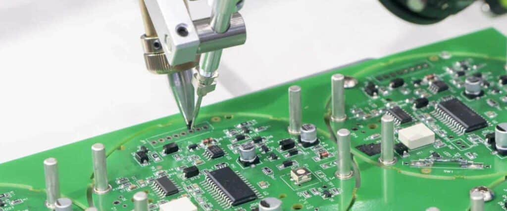
When designing a full wave rectifier, the printed circuit board (PCB) layout is a critical consideration. The PCB layout determines the physical arrangement of the components, their connections, and the routing of electrical signals. A well-designed PCB layout can help to ensure that the circuit operates efficiently, with minimal interference and noise. It can also help to reduce the risk of component failure, and make the circuit easier to troubleshoot and repair if necessary.
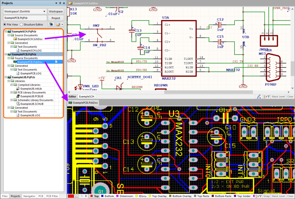
PCB Design Considerations
When designing a full wave rectifier PCB layout, there are several key considerations that must be taken into account to ensure optimal performance. These considerations include component placement, trace routing, and ground plane design.
Component Placement
Proper component placement is critical for a successful full wave rectifier PCB layout. Components should be placed in a logical and organized manner to minimize signal interference and ensure efficient power delivery. Key components such as diodes, capacitors, and resistors should be placed close to each other and as close as possible to the rectifier bridge to minimize trace length and reduce parasitic inductance.
Trace Routing
Trace routing is another important factor to consider when designing a full wave rectifier PCB layout. The goal is to minimize the length of the traces and reduce parasitic inductance and resistance. This can be achieved by using short and direct traces, avoiding sharp corners, and using wide traces for high current paths. It is also important to keep the traces away from sensitive components and to avoid crossing signal paths to prevent signal interference.
Ground Plane Design
Ground plane design is critical to ensure proper grounding and reduce noise in a full wave rectifier PCB layout. A solid ground plane should be used to provide a low impedance return path for the current flow. The ground plane should be connected to the power supply ground and the chassis ground to ensure a common reference point. It is also important to keep the ground plane away from sensitive signal traces to avoid ground loops and reduce noise.
In summary, when designing a full wave rectifier PCB layout, careful consideration should be given to component placement, trace routing, and ground plane design to ensure optimal performance. By following these guidelines, you can ensure a successful design that delivers efficient power and minimal noise.
Full Wave Rectifier Circuit

A full wave rectifier circuit is a type of rectifier that uses both halves of the input waveform to produce a DC output voltage. This circuit is commonly used in power supplies and other applications that require a steady DC voltage.
Circuit Diagram
The circuit diagram for a full wave rectifier is shown below:
The circuit consists of a transformer, four diodes, and a load resistor. The transformer is used to step down the AC voltage from the mains to a lower voltage that can be rectified. The diodes are used to rectify the AC voltage and produce a DC voltage across the load resistor.
Component Selection
When selecting components for a full wave rectifier circuit, it is important to choose components that can handle the voltage and current requirements of the circuit. The transformer should be rated for the input voltage and output voltage required by the circuit. The diodes should be rated for the maximum voltage and current that will be present in the circuit.
Some common diodes used in full wave rectifier circuits are the 1N4001 and the 1N5408. These diodes have a maximum voltage rating of 50V and 1000V, respectively, and a maximum current rating of 1A and 3A, respectively.
The load resistor should be chosen based on the desired output voltage and current of the circuit. The value of the load resistor can be calculated using Ohm’s law and the desired output voltage and current.
In summary, a full wave rectifier circuit is a useful circuit for producing a steady DC voltage from an AC input voltage. When designing this circuit, it is important to select components that can handle the voltage and current requirements of the circuit. The circuit diagram and component selection are the two main aspects of designing a full wave rectifier circuit.
PCB Layout Guidelines
Layout Techniques
When laying out a full wave rectifier PCB, there are several techniques that can be employed to ensure optimal performance. Firstly, it is important to keep the input and output traces as short as possible to minimize parasitic inductance and capacitance. This can be achieved by placing the rectifier as close as possible to the input source and the load.
Secondly, it is recommended to place the rectifier and the filter capacitor on opposite sides of the PCB to minimize the loop area and reduce electromagnetic interference. Additionally, it is important to ensure that the ground plane is continuous and connected to the rectifier and the filter capacitor.
Thirdly, it is recommended to use a star grounding topology, where all the ground connections are brought to a single point, to reduce ground loops and minimize noise.
Signal Integrity Considerations
When designing a full wave rectifier PCB, it is important to consider the signal integrity to ensure that the rectified output signal is free from noise and distortion. One way to achieve this is to use low-impedance traces for the input and output signals and to ensure that the trace width is sufficient to handle the current.
Additionally, it is recommended to use a ground plane to provide a low-impedance return path for the signal and to minimize electromagnetic interference. It is also important to ensure that the input and output traces are routed away from high-frequency sources, such as switching power supplies, to avoid coupling noise into the signal.
In summary, when designing a full wave rectifier PCB, it is important to keep the input and output traces short, use a continuous ground plane, employ a star grounding topology, use low-impedance traces, and consider the signal integrity to ensure optimal performance.
Testing and Troubleshooting
Testing Procedures
To ensure that the full wave rectifier PCB layout is functioning correctly, it is recommended to perform a few testing procedures. Firstly, check the voltage output using a multimeter. The voltage output should be equal to the input voltage minus the voltage drop across the diodes. Secondly, check the ripple voltage using an oscilloscope. The ripple voltage should be within the acceptable range, which is typically less than 5% of the output voltage. Finally, check the power dissipation of the diodes using a power meter. The power dissipation should not exceed the maximum rating of the diodes.
Common Issues and Solutions
There are a few common issues that may arise when testing a full wave rectifier PCB layout. One issue is a high ripple voltage, which may be caused by a faulty capacitor or incorrect capacitor value. To solve this issue, replace the capacitor or use the correct capacitor value. Another issue is a low voltage output, which may be caused by a faulty transformer or incorrect transformer rating. To solve this issue, replace the transformer or use the correct transformer rating. A third issue is a high power dissipation of the diodes, which may be caused by a high input voltage or incorrect diode rating. To solve this issue, reduce the input voltage or use diodes with a higher rating.
Overall, by following the testing procedures and troubleshooting common issues, it is possible to ensure that the full wave rectifier PCB layout is functioning correctly.
