Table of Contents
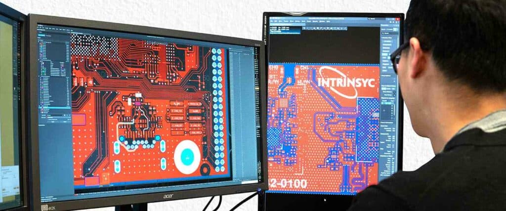
ToggleGraphics card PCB layout is a crucial aspect of graphics card design. The Printed Circuit Board (PCB) is the foundation of the graphics card, and it plays a significant role in determining the card’s performance and stability. The PCB layout is responsible for routing power and signals between various components, including the graphics processing unit (GPU), memory chips, and power delivery subsystems.
The PCB layout is a complex process that involves careful planning and execution. It requires a deep understanding of the electrical and thermal properties of the components, as well as the physical constraints of the graphics card’s form factor. The PCB layout must be optimized to minimize signal interference, reduce power loss, and maximize cooling efficiency. A well-designed PCB can improve the graphics card’s performance, stability, and longevity, while a poorly designed one can lead to issues such as overheating, signal noise, and system crashes.
In this article, we will explore the fundamentals of graphics card PCB layout and delve into some of the key considerations that go into designing a high-performance graphics card. We will examine the various components that make up the PCB, the role of power delivery and thermal management, and the impact of PCB layout on signal integrity and performance. By the end of this article, you will have a better understanding of the importance of PCB layout in graphics card design and the factors that contribute to a successful layout.

Basics of Graphics Card PCB Layout
Components of a Graphics Card PCB Layout
A graphics card PCB layout is made up of various components that work together to provide the necessary functionality. These components include the following:
- GPU (Graphics Processing Unit)
- Memory (VRAM)
- Power Delivery (VRM)
- Display Outputs (HDMI, DisplayPort, etc.)
- Cooling System (Fans, Heatsinks, etc.)
- Control Circuitry (BIOS, Voltage Regulators, etc.)
The GPU is the main component of a graphics card, responsible for processing and rendering graphics. The VRAM provides the memory necessary for storing and accessing data quickly. The power delivery system is responsible for providing the necessary voltage and current to the GPU and VRAM. The display outputs allow for connecting the graphics card to a monitor or other display device. The cooling system is responsible for dissipating the heat generated by the GPU and other components. The control circuitry includes the BIOS and voltage regulators, which provide control and regulation of various functions.
Design Considerations for Graphics Card PCB Layouts
When designing a graphics card PCB layout, there are several key considerations to keep in mind. These include the following:
-
Power Delivery: The power delivery system must be designed to provide the necessary voltage and current to the GPU and VRAM, while also ensuring stability and efficiency.
-
Signal Integrity: The PCB layout must be designed to ensure signal integrity, which involves minimizing noise and interference, and ensuring proper impedance matching.
-
Thermal Management: The cooling system must be designed to dissipate the heat generated by the GPU and other components, while also ensuring proper airflow and temperature control.
-
Form Factor: The PCB layout must be designed to fit within the physical constraints of the graphics card form factor, while also ensuring proper placement and orientation of components.
By considering these key design considerations, graphics card manufacturers can ensure that their products provide optimal performance, stability, and reliability.
Advanced Techniques for Graphics Card PCB Layout

Signal Integrity and Power Integrity for Graphics Card PCB Layouts
Signal integrity and power integrity are two critical aspects of graphics card PCB layout. Signal integrity refers to the ability of the PCB to maintain the integrity of signals as they travel through the circuit. Power integrity, on the other hand, refers to the ability of the PCB to maintain stable power delivery to the components.
To ensure good signal and power integrity, it is important to follow these best practices:
- Use proper ground planes and power planes to reduce noise and interference.
- Place decoupling capacitors close to the power pins of each component to reduce noise on the power supply.
- Use controlled impedance traces for high-speed signals to maintain signal integrity.
- Avoid routing high-speed signals over split planes or through vias, which can cause reflections and signal degradation.
Thermal Management for Graphics Card PCB Layouts
Thermal management is another critical aspect of graphics card PCB layout. Graphics cards generate a lot of heat, and without proper thermal management, the components can overheat and fail.
To ensure good thermal management, it is important to follow these best practices:
- Use a large copper area on the PCB to act as a heatsink for the components.
- Use thermal vias to transfer heat from the components to the copper area.
- Ensure proper airflow through the card by designing the card with proper ventilation.
- Use thermal pads or paste to ensure good thermal contact between the components and the heatsink.
By following these advanced techniques for graphics card PCB layout, designers can ensure good signal and power integrity, as well as proper thermal management, resulting in a high-performance and reliable graphics card.
Testing and Validation for Graphics Card PCB Layouts

Testing Methods for Graphics Card PCB Layouts
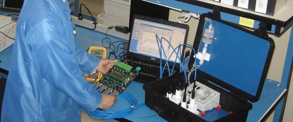
Testing is an essential part of the graphics card PCB layout design process. It helps to ensure that the design meets the required specifications and performs as expected. There are several testing methods that can be used to validate the PCB layout design.
One of the most common testing methods is signal integrity testing. This involves measuring the performance of the signals that run through the PCB. It helps to identify any issues that may cause signal degradation, such as noise, crosstalk, or reflections.
Another testing method is power integrity testing. This involves measuring the performance of the power supply system on the PCB. It helps to identify any issues that may cause power delivery problems, such as voltage drop, noise, or instability.
Thermal testing is also an important part of the testing process. It helps to ensure that the PCB layout can handle the heat generated by the graphics card components. This involves measuring the temperature of the PCB under different operating conditions.
Validation Techniques for Graphics Card PCB Layouts
Validation is the process of verifying that the PCB layout design meets the required specifications and performs as expected. There are several validation techniques that can be used to ensure that the PCB layout design is valid.
One of the most common validation techniques is simulation. This involves using software tools to simulate the behavior of the PCB layout design under different operating conditions. It helps to identify any issues that may cause performance problems, such as timing violations, signal integrity issues, or power delivery problems.
Another validation technique is prototyping. This involves building a physical prototype of the PCB layout design and testing it under different operating conditions. It helps to identify any issues that may not have been detected during simulation, such as mechanical problems or thermal issues.
In conclusion, testing and validation are critical parts of the graphics card PCB layout design process. By using the right testing methods and validation techniques, designers can ensure that the PCB layout design meets the required specifications and performs as expected.

