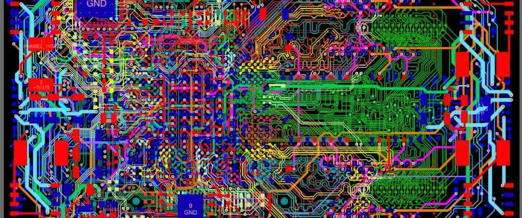
High density PCB design has become increasingly important in the electronics industry. With the miniaturization of electronic devices, the demand for high density PCBs has grown. High density PCBs allow for more components to be placed on a smaller board, resulting in smaller and more efficient devices.
Designing high density PCBs requires careful consideration of various factors. The placement and routing of components, the size and shape of the board, and the materials used all play a crucial role in the success of the design. In addition, high density PCBs often require advanced manufacturing techniques, such as laser drilling and microvia technology. As a result, designing high density PCBs can be a challenging and complex process.
Overview
High density PCB design is an advanced technique that involves placing a large number of components on a small surface area. This technique is used to create complex and high-performance electronic devices that require a high level of integration. In this section, we will discuss what high density PCB design is and the benefits it offers.
What is High Density PCB Design?
High density PCB design is a process that involves placing a large number of components on a small surface area. This is achieved by using advanced techniques such as surface mount technology (SMT), through-hole technology (THT), and multi-layer PCBs. High density PCB design requires careful planning and attention to detail, as any errors can result in significant design problems.
Benefits of High Density PCB Design
There are several benefits to using high density PCB design for electronic devices. One of the primary benefits is that it allows for a high level of integration, which means that more components can be placed on a smaller board. This results in a smaller form factor, which is particularly important for portable devices such as smartphones and tablets.
Another benefit of high density PCB design is that it allows for greater signal integrity. By placing components closer together, the signal paths are shorter, which reduces the risk of interference and signal loss. This is particularly important for high-speed digital circuits, where even small amounts of interference can cause significant problems.
Finally, high density PCB design allows for greater flexibility in design. With more components on a smaller board, designers have more freedom to create complex circuits and devices. This can result in devices that are more efficient, more reliable, and more cost-effective.
In conclusion, high density PCB design is an advanced technique that offers several benefits for electronic devices. By placing a large number of components on a small surface area, high density PCB design allows for a high level of integration, greater signal integrity, and greater flexibility in design.
Design Considerations

When designing high density printed circuit boards (PCBs), there are several important considerations to keep in mind. These include component placement, trace routing, via placement, and power and ground planes.
Component Placement
Component placement is a critical aspect of high density PCB design. It is important to carefully consider the placement of each component to ensure that the board is compact and efficient. Some tips to keep in mind when placing components include:
- Group components together based on their function
- Place components in a way that minimizes the length of traces
- Consider the heat generated by each component and ensure that they are spaced appropriately
- Place components in a way that allows for easy access for testing and maintenance
Trace Routing
Trace routing is another important consideration in high density PCB design. The goal is to minimize the length of traces while ensuring that they are not too close together. This can be accomplished by:
- Using a grid system to ensure that traces are aligned
- Routing traces in a way that minimizes the number of vias required
- Using differential pairs for high-speed signals
- Keeping traces away from sensitive components and high heat areas
Via Placement
Vias are an essential part of high density PCB design, as they allow for the connection of different layers of the PCB. When placing vias, it is important to:
- Use as few vias as possible
- Place vias in a way that minimizes the length of traces
- Ensure that vias are spaced appropriately to avoid signal interference
- Consider the size of the via and the current that will be passing through it
Power and Ground Planes
Power and ground planes are critical for high density PCB design, as they provide a stable and reliable power source for the board. When designing power and ground planes, it is important to:
- Use a solid plane for both power and ground
- Ensure that the power and ground planes are connected by multiple vias
- Place decoupling capacitors as close to the power pins of each component as possible
- Consider the thickness of the power and ground planes based on the current that will be passing through them
By keeping these design considerations in mind, you can create a high density PCB that is compact, efficient, and reliable.
Manufacturing Considerations

When designing a high-density PCB, there are several manufacturing considerations that must be taken into account to ensure that the final product is of high quality and reliability. These considerations include materials selection, assembly process, testing, and inspection.
Materials Selection
Materials selection is a critical aspect of high-density PCB design. The materials used must be able to withstand the high temperatures and pressures that are involved in the manufacturing process. Some of the key materials used in high-density PCBs include copper, aluminum, and various types of plastics. It is important to select materials that are able to withstand the stresses of the manufacturing process and that are also able to meet the electrical and thermal requirements of the final product.
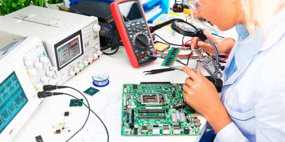
Assembly Process
The assembly process for high-density PCBs is also a critical factor in ensuring the quality and reliability of the final product. The assembly process involves the placement of components onto the PCB and the soldering of these components to the board. This process must be performed with precision and accuracy to ensure that the components are properly aligned and that the solder joints are strong and reliable. The use of automated assembly equipment can help to improve the accuracy and consistency of the assembly process.
Testing and Inspection
Testing and inspection are also critical aspects of high-density PCB manufacturing. Testing is used to ensure that the PCB meets the electrical and thermal requirements of the final product. Inspection is used to identify any defects or problems with the PCB that may impact its performance or reliability. There are several different types of testing and inspection methods that can be used, including X-ray inspection, optical inspection, and functional testing.
In summary, when designing a high-density PCB, it is important to consider the materials selection, assembly process, testing, and inspection to ensure that the final product is of high quality and reliability. By paying careful attention to these factors, it is possible to create a high-density PCB that meets the requirements of the final product and that is able to withstand the stresses of the manufacturing process.
Design Tools

When designing high density PCBs, it is important to have the right design tools. The following subsections discuss two essential design tools: CAD software and simulation tools.
CAD Software
CAD software is an essential tool for high density PCB design. It allows designers to create schematic diagrams and PCB layouts quickly and accurately. Some popular CAD software for high density PCB design include:
- Altium Designer
- Eagle PCB Design
- KiCad
Each CAD software has its own strengths and weaknesses, so it is important to choose the one that best fits your needs and budget.
Simulation Tools
Simulation tools are another essential tool for high density PCB design. They allow designers to simulate and test their designs before manufacturing, saving time and money. Some popular simulation tools for high density PCB design include:
- SPICE
- LTspice
- PSpice
Simulation tools can simulate various aspects of the design, such as signal integrity, power integrity, and thermal management. They can also help identify potential problems and optimize the design for performance.
In conclusion, having the right design tools is crucial for high density PCB design. CAD software and simulation tools are two essential tools that can help designers create accurate and optimized designs.
Future Trends
As technology continues to advance, the world of high density PCB design is constantly evolving. Here are a few trends to keep an eye on in the future:
-
Miniaturization: As devices become smaller and more compact, the demand for high density PCBs will only increase. PCB designers will need to find new ways to pack more components onto smaller boards without sacrificing functionality or reliability.
-
Advanced Materials: New materials such as flexible PCBs and 3D printed PCBs are becoming increasingly popular. These materials offer unique advantages such as improved flexibility, reduced weight, and increased durability.
-
Increased Automation: With the rise of AI and machine learning, it’s likely that more aspects of PCB design will become automated in the future. This could lead to faster design times, reduced errors, and increased efficiency.
-
Improved Testing and Validation: As high density PCBs become more complex, it’s becoming increasingly important to thoroughly test and validate designs before they are manufactured. New testing and validation techniques are being developed to ensure that PCBs meet the highest standards of quality and reliability.
Overall, the future of high density PCB design looks bright. With new materials, advanced automation, and improved testing and validation techniques, designers will be able to create smaller, more powerful, and more reliable PCBs than ever before.
