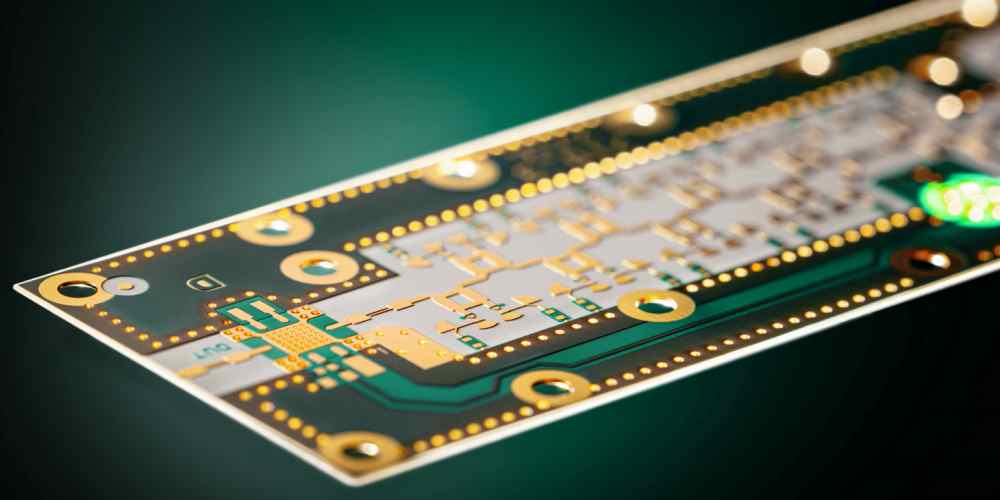
High frequency Printed Circuit Boards, also called HF PCBs, are the circuit boards used for the high-powered applications. They became popular following the ever-increasing complexity, due to the improved designs of electronic components.
If you are to work on a high frequency PCB design, it has to follow the right guidelines. It is also imperative to use the right materials and work with a reliable PCB manufacturer.
What are High Frequency PCBs?
These are the circuit boards that operate at a higher frequency. They also the ideal type of PCB for the complex electronic components that require faster signal transmission. The speed of transmitting signals within the board is one major attribute of this type of PCB.
How are Signals Transmitted?
Signal transmission in high frequency PCBs is done in the form of electromagnetic waves, measured in the frequency of GHz.
The following are additional pieces of information you need to know about how signals are transmitted in high frequency circuit boards:
1. Frequency Range
The fact that the frequency is higher doesn’t end at the speed of transmitting signals. The high frequency PCBs potentially have a range of 24 to 100 GHz.
2. Special Signal Provisions
Using the HF PCBs is a great addition to the signal flow in consumer electronics. This became a necessity, following the increased signal flow rates required from the complex electronic switches. In addition to meeting those demands, these PCBs also allow for the integration of special signal requirements into the electronic products and devices.
3. Balancing Signal Flow with Pulse Rising Times
Due to the shorter pulse rising times in consumer electronics, it has become imperative that the high frequency technology is used to resolve the issue.
The resolution comes in the form of taking or treating the conductor widths as an electronic component for the PCB. This consideration enables the integration of the conductor widths into the fold, and using that to balance the pulse rising times.
High Frequency PCB Materials: Which Ones are the Best?
When it comes to the selection of the best materials for high frequency circuit boards, the priority is on those laminates that assure of faster signal transmission.
Several other factors, if carefully put into perspective, can also influence the choice of such laminates.
Here are some of the things you need to know about choosing your high frequency laminates:
1. Specific Manufacturers
The best laminates for HF PCBs are sourced from particular manufacturers. If you don’t do this, you might end up buying sub-standard materials.
The list of manufacturers that make the best laminates includes the following brands:
- Rogers
- Taconic
- Isola
- Megtron by Panasonic and;
- Teflon
2. Variances in Materials
You will notice that some of the materials vary, in terms of their performances. This is so because of the disparities, arising from the environment/application and the signal transmission speeds.
3. Survivability and Adaptation
It is one thing to pick a high frequency laminate and another for the same to meet the needs of the immediate environment. In this regard, it might be impossible to achieve a sustainable survivability and adaptation of the materials if they are not meant for the particular application.
For context, you will achieve greater circuit board materials’ adaptation, survivability and increased water absorption capabilities if you go for the flexible circuits. You can also use the new-generation and Teflon substrates to achieve the same purpose.
4. FR-4 vs. Teflon Substrates
If you are to choose between the Flame Retardant 4 (FR-4) materials and the Teflon substrates/materials, it has to be based on the performances.
For context, the FR-4 materials, asides from being one of the most-popular substrates, also costs less than the newer generation substrates, such as Teflon and Flex circuits.
However, the best way to get the most out of the FR-4 materials is by using an appropriate layer buildup.
On the downside, the FR-4 material might not be the best option, due to the possible drop in performance, once it edges close to a signal speed of 1.6 GHz.
On the other hand, the newer generation substrates, such as Teflon and Flex offer improved signal rate, usually higher than FR-4 material’s 1.6 GHz. In addition to offering lower dielectric constant, and low-loss factor, these materials also offer up to 10 GHz of frequency.
The downside to the newer generation HF PCB materials is that they are more expensive, than the FR-4 PCB materials.
5. High Frequency PCB’s Special Material Requirements
The types of materials or substrates used for making this type of PCB must be special. Some of the specific requirements made in this regard, include:
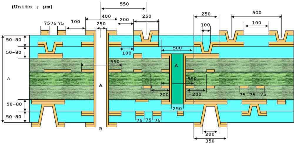
- Homogenous Construction: this also comes with low tolerances, especially for the dielectric constant and insulation thickness.
- Adapted permittivity and;
- Low attenuation, used for the excellent signal transmission on the circuit board.
Which is the Best HF PCB Material?

With several options out there, sometimes, choosing the best material for your high frequency PCB can pose a challenge. Nevertheless, we will point out in this section, some of the key upsides and downsides to some of the common materials used for the design.
Teflon Materials
Also known as Polyfluoretraethylene (PTFE), Teflon is one of the HF PCB materials you can use for higher applications. With the frequencies ranging up to 10 GHz, you can be sure of using it to satiate the needs of the applications that require as much as that frequency.
On the flip side, you will find the PTFE/Teflon high frequency PCB material difficult to use because of the following reasons:
- A special surface treatment option is required, due to the molecule inertia of the PTFE material.
- Heat resistance is not top-notch and that is best-balanced with the use of either fiberglass or several Si02 as the filing material.
FR-4 Materials
You can consider using the FR-4 materials due to the affordability. You can also count on it as a solid laminate material for the HF PCBs, due to the excellent performance in hybrid circuit board constructions. In this instance, the FR-4 material is combined with the HF PCB’s laminate to bolster the hybrid design.
Therefore, the core differences between the PTFE/Teflon and FR-4 materials are the costs and overall performance. Although the Teflon material is costlier, it delivers maximum signal transmission rates, up to 10 GHz. This is better than the less than 2 GHz signal flow in the FR-4 material.
High Frequency PCB Properties
What and what makes up the overall design of the high frequency circuit boards? The following are some of the features:
1. Lower Moisture Absorption
Increasing the rate at which signal flows in the board is one benefit of this material. The other is the lower rate at which it is exposed to water. This makes it less susceptible to damage, especially when exposed or used in humid environments.
2. Lower Dimensional Stability
It is possible for a PCB, especially the one that transmits signals at a fast pace, to expand or get compressed.
Due to the low dimensional stability, the high frequency PCBs maintain the original sizes, irrespective of the temperature or environment they are being used.
3. Smaller DF
HF PCBs are known to have a lower DF, which stands for Dissipation Factor. This refers to the rate at which the heat dissipation operates – and which doesn’t negate the signal transmission speeds.
With the Dissipation Factor (DF) ranging between 0.0019 and 0.025, you can be sure that the quality of the signal wouldn’t be affected, negatively. On the contrary, a lower DF is a major boost to the boost to the signal transmission rate, as it reduces the chances/incidences of signal loss.
4. Chemical Resistance
Faster signal speeds are not all that the HF PCBs offer. They also withstand exposures to chemicals, whereby the circuit boards wouldn’t be damaged or start malfunctioning due to the exposure to chemicals.
5. HF PCBs have Lower DKs
DKs refer to the Dielectric Constants. High frequency circuit boards are known to have lower and stable DKs.
A lower or lesser dielectric constant is a win as it prevents the board from suffering delays during signal transmission. The lowered DK helps to bolster signal transmission, and at a stabilized pace.
How to Make a High-Quality PCB for Signal Transmission
You can make your high frequency circuit board to boost signal transmission, by using the ideal fabrication process. These processes include:
1. Design the PCB
Your first step is to make a design of the HF PCB. Use circuit board software like EAGLE, KiCAD EDA, and EasyEDA to make the design.
2. Print the Design
You should now use a plotter printer to print-out the design. Note that there are two inks visible on the design/PCB film. The first is the black ink that denotes the copper and the other is the clear ink, used to mark the non-conductive parts of the circuit board.
3. Start Copper-Printing
Once the PCB has been imprinted on the laminate, the next step is to pre-bond the copper on the laminate that serves as the PCB’s structure.
4. Layers’ Alignment
You now need to align the layers or position them in the right way. This process often requires drilling holes into the inner and outer layers of the board.
5. Join the Layers
Join or laminate the layers, by way of using a metal clamp to join them. The clamp should only be used to join the inner and outer layers, after they have been layered-up.
6. Drilling and Plaiting the PCB
Your next line-of-action is to drill holes in the board, as a way of securing it. Once this is done, you can start plaiting the board, with the aid of chemicals.
Make sure the board’s surface is cleaned, before applying the chemicals to sandwich the PCB’s layers.
7. Apply the Solder Mask
You can now apply the solder mask on the circuit’s surface. Both the solder film and epoxy ink will be used for the process.
8. Silkscreen the PCB
The silkscreen must now be applied to boost the board’s protection. It must be applied, only after the board has been plated with any of the following – Gold, HASL or Silver.
9. HF PCB Testing
At Hillman Curtis, we subject your high frequency Printed Circuit Board to testing. This helps us find out if the board functions, as it is expected to do.
10. Cut the HF PCB
Cuttings can be done with the aid of a V-groove process of a CNC machine.
General High Frequency PCB Design Guidelines to Follow
Want to get the most out of the signal flow in your HF PCB? If so, you must follow some of the best practices or certified high power PCB design guidelines.
These are some of the guidelines:
1. Determine the Signal Frequency
Despite the fact that the PCB can facilitate the flow of signals, it is also imperative to be sure that all things are in the way they should be.
Determining the signal frequency requires making plans on reducing noise dissipation during signal transmission. It also requires deciding between dividing the power planes, balancing the minimal tolerances and checking the possibility of integrating several signals.
2. Frequency Signals must be Routed
It is imperative to have the frequency signals routed. This enables the usage of different signal routing processes, such as:
- Applying the 20H Rule to reduce plane decoupling.
- Creating a route for the frequency signal, starting from the source and ending at the sink via the path.
- Using the 3W Rule to reduce the chances of plane coupling.
3. Your HF PCB Design Comes First
The design is a blueprint or an outlook of what your high frequency PCB is expected to look like. You are required to have an idea of what type of board design to make and the necessary integrations to be made.
We can help you figure out the best design paths so you don’t have to brainstorm that much.
Final Words
The high frequency circuit boards solve one major challenge holding down many PCBs from performing as they should – low signal transmission. By boosting the signal transmission rate, you can be sure that your next circuit board projects will reduce excessive heat dissipation, reduce chemical infiltration and offer an improved signal transmission rate that results in well-performing Printed Circuit Boards (PCBs).
