IPC, or the Institute for Printed Circuits, is an international organization that sets standards for the design and manufacture of printed circuit boards (PCBs). IPC standards cover a variety of topics related to PCB design, including materials, fabrication processes, and quality control. One of the most important aspects of PCB design is ensuring that the board meets IPC standards for interconnect reliability, which is critical for the performance and longevity of electronic devices.
IPC standards for PCB design are constantly evolving to keep up with advances in technology and changes in industry needs. For example, the IPC-2221 standard provides guidelines for the design of PCBs with high-speed signals, while the IPC-4101 standard covers the properties of various laminate materials used in PCB fabrication. By adhering to IPC standards, designers and manufacturers can ensure that their PCBs meet the highest levels of quality and reliability, and that they are compatible with other components and systems.
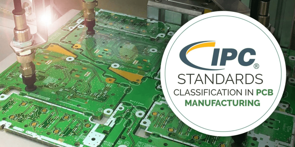
IPC Standards
When designing printed circuit boards (PCBs), following the standards set by the Institute for Printed Circuits (IPC) is crucial. The IPC is a global trade association that develops and publishes standards for the design, manufacture, and testing of PCBs.
IPC-2221A
IPC-2221A is the generic standard for PCB design. It provides guidelines for the design of PCBs and includes information on material selection, board thickness, and trace width. It also covers requirements for layer count, hole sizes, and component placement.
One of the key aspects of IPC-2221A is its focus on standardization. By following the guidelines set forth in this standard, PCB designers can ensure that their boards will be compatible with a range of manufacturing processes and components.
IPC-2222
IPC-2222 is a standard for the design of high-density interconnect (HDI) PCBs. HDI PCBs are used in devices that require a high level of functionality in a small form factor, such as smartphones and tablets.
IPC-2222 provides guidelines for the design of HDI PCBs, including information on layer stacking, via placement, and trace routing. It also covers requirements for material selection, board thickness, and component placement.
By following the guidelines set forth in IPC-2222, designers can ensure that their HDI PCBs will meet the requirements for high-speed, high-density applications.
Overall, IPC standards are essential for ensuring that PCBs are designed to meet the requirements of a range of manufacturing processes and applications. By following these standards, designers can ensure that their boards are reliable, efficient, and compatible with a range of components and manufacturing processes.
IPC Footprint Naming Convention

When designing a PCB, it’s essential to use the right footprint for each component. The IPC (Institute for Printed Circuits) has developed a standard naming convention for footprints to ensure consistency and accuracy across the industry.
The IPC naming convention consists of a series of letters and numbers that indicate the component type, size, and number of pins. The letters represent the component type, while the numbers represent the size and number of pins.
For example, a resistor with two pins and a 1206 package size would have the following IPC footprint name: R_1206_2.
Here’s a breakdown of the IPC footprint naming convention:
- The first letter represents the component type. For example, “R” for resistor, “C” for capacitor, “U” for integrated circuit, and so on.
- The second and third letters represent the package size. For example, “0402” for a small resistor or capacitor, “1206” for a larger one, and so on.
- The fourth and fifth numbers represent the number of pins. For example, “2” for a two-pin component, “4” for a four-pin component, and so on.
It’s important to note that not all components will have an IPC footprint name. Some components may have unique footprints that are not covered by the standard naming convention. In these cases, it’s best to consult the component datasheet or contact the manufacturer for guidance.
By using the IPC footprint naming convention, PCB designers can ensure that they are using the correct footprint for each component. This helps to prevent errors and ensure that the PCB functions as intended.
IPC Footprint Design
When designing a printed circuit board (PCB), it is crucial to follow industry standards to ensure the reliability and manufacturability of the board. The Institute of Printed Circuits (IPC) provides guidelines for various aspects of PCB design, including footprint design.
Padstack Design
The padstack design is an essential part of the PCB footprint. It defines the size, shape, and spacing of the pads that connect the PCB to other components. The IPC provides guidelines for padstack design, including minimum and maximum dimensions, tolerances, and recommended shapes.
When designing the padstack, it is essential to consider the size and pitch of the component’s leads or pins. The pad size should be large enough to provide sufficient solder fillet and thermal relief. The spacing between pads should be wide enough to prevent solder bridging but not so wide that it affects the signal integrity.
Trace Width and Spacing
The trace width and spacing are also critical factors in the PCB footprint design. The IPC provides guidelines for trace width and spacing based on the current carrying capacity and the voltage level of the circuit. The wider the trace, the higher the current it can carry without overheating. The spacing between traces should be wide enough to prevent electrical interference or crosstalk.
When designing the PCB footprint, it is essential to consider the manufacturing process and the capabilities of the PCB manufacturer. The design should be optimized for the manufacturing process, and the manufacturer’s capabilities should be considered when selecting the trace width and spacing.
In conclusion, following the IPC guidelines for footprint design is crucial for ensuring the reliability and manufacturability of the PCB. The padstack design and trace width and spacing are critical factors that should be carefully considered during the design process.
IPC Footprint Verification

When designing a printed circuit board (PCB), it is essential to ensure that the footprints of the components are accurate. This is where IPC Footprint Verification comes in. IPC Footprint Verification is a process that verifies that the dimensions of the footprint of a component match the dimensions specified in the IPC standard.
Footprint Verification Checklist
To ensure that the footprints of the components are accurate, the following checklist can be used:
- Verify the pad dimensions, including the length, width, and thickness
- Check the pitch of the pins
- Check the position of the pins
- Verify the orientation of the component
- Check the silkscreen markings
Footprint Verification Tools
There are several tools available to verify the footprints of the components:
-
IPC-7351 Footprint Calculator: This tool calculates the recommended footprint dimensions for a component based on the IPC-7351 standard.
-
Footprint Verification Software: There are several software tools available that can verify the footprints of the components. These tools compare the dimensions of the footprint with the dimensions specified in the IPC standard.
-
Automated Optical Inspection (AOI): AOI is a process that uses optical cameras to inspect the PCB for defects. This process can also be used to verify the footprints of the components.
In conclusion, IPC Footprint Verification is an essential process in PCB design. By following the Footprint Verification Checklist and using the appropriate tools, designers can ensure that the footprints of the components are accurate, which can help to prevent errors and reduce costs.
IPC Footprint Management

When designing a printed circuit board (PCB), it is essential to ensure that the components are accurately placed and connected. The IPC (Institute of Printed Circuits) has established industry standards for PCB design, including guidelines for creating and managing footprints.
Footprint Library Management
A footprint library is a collection of pre-designed component footprints that can be used in PCB design. Managing the library is crucial to ensure that the footprints are up-to-date and accurate. It is recommended to use a version control system to keep track of changes and updates to the library. This helps to ensure that the correct footprint is used for each component and that there are no errors in the design.
Footprint Creation and Modification
Creating and modifying footprints is an essential part of PCB design. It is essential to ensure that the footprint is accurate and matches the component’s physical dimensions. When creating or modifying a footprint, it is crucial to refer to the component datasheet and IPC standards to ensure that the footprint is correct.
When creating a new footprint, it is recommended to follow the IPC footprint naming convention. This convention ensures that the footprint name accurately reflects the component’s physical dimensions and pin configuration. It is also essential to ensure that the footprint has the correct pad sizes and spacing to ensure that the component is correctly placed and soldered onto the PCB.
In conclusion, managing and creating footprints is a crucial part of PCB design. Following IPC standards and guidelines ensures that the footprints are accurate and up-to-date, reducing the risk of errors in the design.
