KiCad is a free and open-source software suite used for electronic design automation (EDA). It is a popular tool for designing printed circuit boards (PCBs) and is used by hobbyists, students, and professionals alike. KiCad is available on multiple platforms, including Windows, macOS, and Linux, and has a user-friendly interface that makes it easy to use.
KiCad offers a range of features that make it a powerful tool for designing PCBs. It includes a schematic editor, a PCB layout editor, and a 3D viewer. The schematic editor allows users to create and edit electronic schematics, while the PCB layout editor lets users create and edit PCB layouts. The 3D viewer allows users to view their designs in 3D, which can help identify potential issues before the PCB is manufactured.
Overall, KiCad is a versatile and powerful tool for designing PCBs. Its user-friendly interface and range of features make it an excellent choice for hobbyists, students, and professionals who want to create high-quality PCB designs.

KiCad Design Process
KiCad is a free and open-source software suite used for electronic design automation (EDA). The software includes tools for schematic capture, PCB layout design, and more. The KiCad design process typically involves four main stages: schematic capture, footprint creation, PCB layout design, and design rule check (DRC).
Schematic Capture
The first step in the KiCad design process is schematic capture. This involves creating a schematic diagram of the electronic circuit you want to design. KiCad provides an intuitive schematic editor that allows you to create and edit your schematic diagram. You can add components, connect them with wires, and label them appropriately.
Footprint Creation
After creating the schematic diagram, the next step is to create footprints for the components used in the design. Footprints are physical representations of the components that will be used in the PCB layout. KiCad provides a built-in footprint editor that allows you to create custom footprints or modify existing ones.
PCB Layout Design
Once you have created the schematic diagram and footprints, the next step is to design the PCB layout. KiCad provides a comprehensive PCB layout editor that allows you to place components, route traces, and add copper pours. You can also add text, graphics, and other design elements to your PCB layout.
Design Rule Check (DRC)
The final step in the KiCad design process is the design rule check (DRC). This involves checking the design against a set of predefined design rules to ensure that it meets the required specifications. KiCad provides a powerful DRC tool that allows you to check your design for errors, such as overlapping traces, incorrect clearances, and more.
In conclusion, the KiCad design process involves four main stages: schematic capture, footprint creation, PCB layout design, and design rule check (DRC). KiCad provides a comprehensive set of tools for each stage of the design process, allowing you to create high-quality electronic circuits and PCB layouts with ease.
KiCad Software Tools
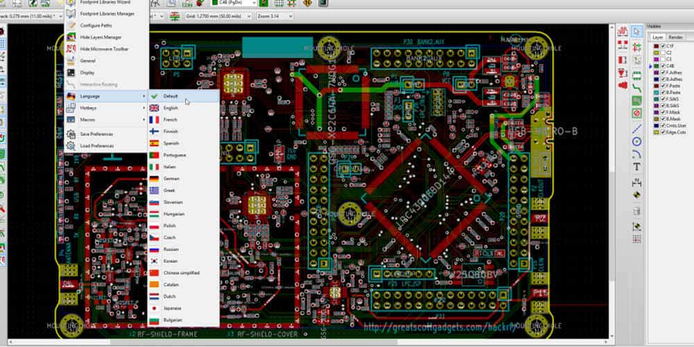
KiCad is an open-source software suite that provides a complete set of tools for designing printed circuit boards (PCBs). The software is available for Windows, Linux, and macOS, and it is constantly being updated by a community of developers.
Eeschema
Eeschema is the schematic editor tool in KiCad. It allows you to create and edit schematic diagrams, which are the blueprints for your PCB design. With Eeschema, you can add components, connect them with wires, and annotate your design with useful information such as part numbers and values.
Some of the features of Eeschema include:
- Hierarchical schematics
- Multiple sheets per schematic
- Automatic netlist generation
- BOM generation
- Customizable keyboard shortcuts
Pcbnew
Pcbnew is the PCB layout editor tool in KiCad. It allows you to place components, route traces, and define copper pours to create your final PCB design. With Pcbnew, you can also perform design rule checks (DRC) to ensure that your design meets your specific manufacturing requirements.
Some of the features of Pcbnew include:
- Interactive routing
- Differential pair routing
- 3D visualization
- Copper pour management
- Design rule checking (DRC)
Gerbview
Gerbview is the Gerber viewer tool in KiCad. It allows you to view and verify your Gerber files, which are the industry-standard files used by PCB manufacturers to produce your PCB design. With Gerbview, you can also export your Gerber files to send to your manufacturer.
Some of the features of Gerbview include:
- Layer management
- Zoom and pan controls
- Measurement tools
- Image export options
Overall, KiCad provides a comprehensive set of software tools for designing PCBs. With Eeschema, Pcbnew, and Gerbview, you can create your schematic, layout your PCB, and verify your design with ease.
KiCad Libraries

KiCad is an open-source software suite for electronic design automation (EDA) that includes tools for schematic capture, PCB layout, and 3D visualization. KiCad libraries are collections of pre-made components that can be used to speed up the design process. The software comes with a default set of libraries, but users can also create their own libraries or download libraries from the internet.
Schematic Symbols Library
The schematic symbols library contains pre-made symbols for electronic components such as resistors, capacitors, and transistors. These symbols can be placed on the schematic editor canvas to create a visual representation of the circuit. KiCad comes with a default set of schematic symbols, but users can create their own symbols or download symbols from the internet.
Footprints Library
The footprints library contains pre-made footprints for electronic components such as surface-mount devices (SMDs) and through-hole components. These footprints can be used to create the physical layout of the PCB. KiCad comes with a default set of footprints, but users can create their own footprints or download footprints from the internet.
3D Models Library
The 3D models library contains pre-made 3D models for electronic components. These models can be used to create a 3D visualization of the PCB. KiCad comes with a default set of 3D models, but users can create their own models or download models from the internet.
In summary, KiCad libraries are an essential part of the design process, and they can save designers a lot of time and effort. With KiCad’s default libraries and the ability to create custom libraries or download libraries from the internet, designers have access to a vast collection of pre-made components that can be used to create high-quality designs.
KiCad Workflow
Project Creation
To begin a new project in KiCad, select “File” and then “New Project” from the menu. Next, choose a project name and location for the project files. Once the project is created, the next step is to create a schematic.
Schematic Design
To create a schematic in KiCad, select “File” and then “New Schematic” from the menu. From here, you can add components to the schematic by selecting them from the library and placing them on the schematic sheet. Connect the components with wires and add any necessary labels or annotations.
Footprint Assignment
After the schematic is complete, the next step is to assign footprints to the components in the schematic. This can be done by selecting “Tools” and then “Assign Footprints” from the menu. Here, you can select the appropriate footprint for each component in the schematic. It’s important to make sure that the footprints match the physical components that will be used in the final PCB.
PCB Layout
With the footprints assigned, the next step is to create the PCB layout. This can be done by selecting “Tools” and then “Create PCB from Schematic” from the menu. From here, you can arrange the components on the PCB and route the traces between them. It’s important to follow good PCB layout practices to ensure that the final board is functional and reliable.
Gerber Generation
Once the PCB layout is complete, the final step is to generate the Gerber files that will be used to manufacture the PCB. This can be done by selecting “File” and then “Plot” from the menu. From here, you can select the layers to include in the Gerber files and generate them for submission to a PCB manufacturer.
By following this workflow, you can create high-quality PCB designs using KiCad.
