Micro SD cards are a type of removable flash memory card that are widely used in smartphones, tablets, and other portable devices. They are small in size, but can store a large amount of data, making them a popular choice for users who need to store and transfer files on the go. The printed circuit board (PCB) layout of a micro SD card is an important aspect of its design, as it determines the card’s electrical and mechanical properties.
The PCB layout of a micro SD card consists of several layers of copper traces, vias, and pads that are used to connect the card’s components together. These components include the memory chips, controller, and other support circuitry. The layout must be carefully designed to ensure that the card meets industry standards for data transfer rates, power consumption, and reliability.
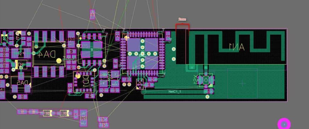
Micro SD Card PCB Layout Design
When designing a printed circuit board (PCB) for a micro SD card, it is important to consider the layout of the card’s pins and the placement of components. The pins of the micro SD card are arranged in a specific order, and it is crucial to ensure that they are connected to the correct traces on the PCB.
One of the most important considerations when designing a micro SD card PCB layout is to ensure that the card is properly grounded. This can be achieved by connecting the ground pins of the micro SD card to the ground plane of the PCB. It is also important to ensure that the power supply pins are connected to the appropriate power supply rails on the PCB.
Another important consideration when designing a micro SD card PCB layout is to ensure that the traces are properly routed. The traces should be kept as short as possible to minimize signal loss and interference. It is also important to ensure that the traces are properly spaced to prevent crosstalk.
When designing a micro SD card PCB layout, it is also important to consider the placement of other components on the board. It is recommended to keep the micro SD card away from other high-speed signals to prevent interference. Additionally, it is important to ensure that the micro SD card is not placed near any heat-generating components to prevent damage to the card.
In summary, when designing a micro SD card PCB layout, it is important to consider the pin layout of the card, the placement of components, the routing of traces, and the grounding of the card. By following these guidelines, designers can ensure that their micro SD card PCB layout is optimized for performance and reliability.
Factors to Consider in Micro SD Card PCB Layout Design

When designing a PCB layout for a micro SD card, there are several important factors to consider. These factors include:
1. Signal Integrity
Signal integrity is crucial in any PCB design, but it is especially important when it comes to micro SD cards. The signals that are transmitted between the micro SD card and the host device must be clean and free from noise. To ensure signal integrity, it is important to minimize the length of the traces, reduce the number of vias, and use proper grounding techniques.
2. Power Supply
The power supply for the micro SD card must be stable and free from noise. The voltage levels must also be within the specified range. It is important to use proper decoupling capacitors and ensure that the power supply traces are as short as possible.
3. EMI/EMC
Electromagnetic interference (EMI) and electromagnetic compatibility (EMC) are important considerations when designing a PCB layout for a micro SD card. To minimize EMI, it is important to use proper grounding techniques, reduce the length of the traces, and use proper shielding. To ensure EMC, it is important to follow the guidelines provided by the micro SD card manufacturer.
4. Placement and Orientation
The placement and orientation of the micro SD card on the PCB can have a significant impact on its performance. It is important to place the micro SD card in an area of the PCB that is free from noise and interference. The orientation of the micro SD card should also be carefully considered to ensure that it is properly aligned with the host device.
By considering these factors, designers can ensure that their PCB layout for a micro SD card is optimized for performance and reliability.
Micro SD Card PCB Layout Design Best Practices
When designing a printed circuit board (PCB) for a micro SD card, there are several best practices to keep in mind. These practices will ensure that the PCB is optimized for performance, reliability, and manufacturability.
Keep Traces Short and Wide
One of the most important considerations when designing a PCB for a micro SD card is the length and width of the traces. The traces should be kept as short as possible to minimize signal loss and noise. Additionally, the traces should be made as wide as possible to reduce resistance and increase current-carrying capacity.
Use Proper Grounding Techniques
Proper grounding is essential for ensuring that the micro SD card operates correctly. Grounding should be done using a solid ground plane, which provides a low-impedance path for returning signals to the source. Additionally, decoupling capacitors should be placed as close as possible to the power pins of the micro SD card to reduce noise and voltage fluctuations.
Minimize Crosstalk
Crosstalk can occur when signals on adjacent traces interfere with each other. To minimize crosstalk, the traces should be routed as far apart as possible. Additionally, traces that carry high-speed signals should be routed on separate layers to reduce interference.
Follow Manufacturer Guidelines
When designing a PCB for a micro SD card, it is important to follow the manufacturer’s guidelines and recommendations. These guidelines will provide information on recommended trace widths, clearance distances, and other design parameters that are specific to the micro SD card being used.
By following these best practices, designers can ensure that their PCBs for micro SD cards are optimized for performance, reliability, and manufacturability.
Common Mistakes in Micro SD Card PCB Layout Design
Designing a printed circuit board (PCB) for a micro SD card can be a challenging task. There are several factors to consider, such as the placement of the components, the routing of the traces, and the selection of the materials. Here are some common mistakes that designers make when creating a PCB layout for a micro SD card.
1. Insufficient Ground Plane
One of the most common mistakes in micro SD card PCB layout design is the lack of a sufficient ground plane. The ground plane is essential for providing a stable reference voltage for the microcontroller and other components on the PCB. Without a proper ground plane, there can be noise and interference, which can affect the performance of the micro SD card.
2. Improper Trace Routing
Another common mistake is improper trace routing. The traces that connect the micro SD card to the rest of the circuit should be kept as short as possible and should be routed away from noisy components. If the traces are too long or are routed too close to other components, there can be signal loss, noise, and interference.
3. Incorrect Component Placement
The placement of the components on the PCB is critical for the performance of the micro SD card. If the components are placed too close together, there can be interference and crosstalk. If the components are placed too far apart, there can be signal loss and noise. It is essential to follow the manufacturer’s guidelines for component placement and to ensure that there is enough space between the components.
4. Inadequate Power Supply
The micro SD card requires a stable power supply for proper operation. If the power supply is inadequate, there can be voltage fluctuations, which can affect the performance of the micro SD card. It is essential to use a stable power supply and to ensure that the voltage regulators are properly designed and placed.
5. Poor Thermal Management
The micro SD card can generate heat during operation, which can affect its performance. It is essential to provide adequate thermal management for the micro SD card, such as proper heat sinking or ventilation. If the micro SD card overheats, it can cause damage to the components and affect the performance of the circuit.
In conclusion, designing a PCB layout for a micro SD card requires careful consideration of various factors. By avoiding these common mistakes, designers can ensure that the micro SD card performs optimally and reliably.
