Micro USB PCBs are a popular choice for a wide range of electronic devices. Many devices such as smartphones, tablets, and other portable devices have micro USB PCB. The design of these PCBs provides a connection between the device and a power source or other peripherals. This structure allows the transfer of data and charging of the device. In this article, we will explore the basics of micro USB PCBs, including their history, design, and key features.
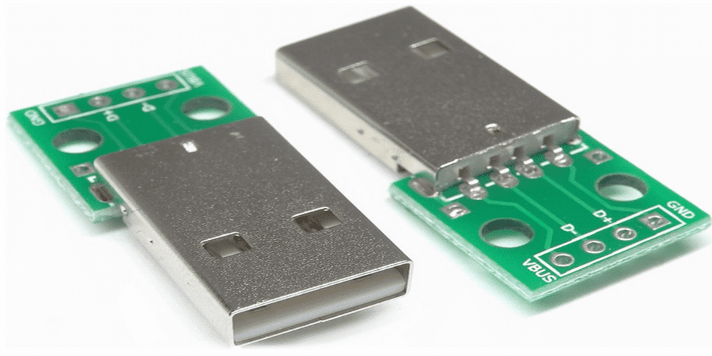
The Micro USB standard was first introduced in 2007. It was a smaller and more durable replacement for the Mini USB connector. Since then, it has become the de facto standard for charging and data transfer in portable electronic devices. Micro USB PCBs feature a standard 5-pin layout, with four pins for data transfer and one pin for charging. The compact size of the connector allows for its use in smaller devices. This arrangement makes it an ideal choice for portable electronics.
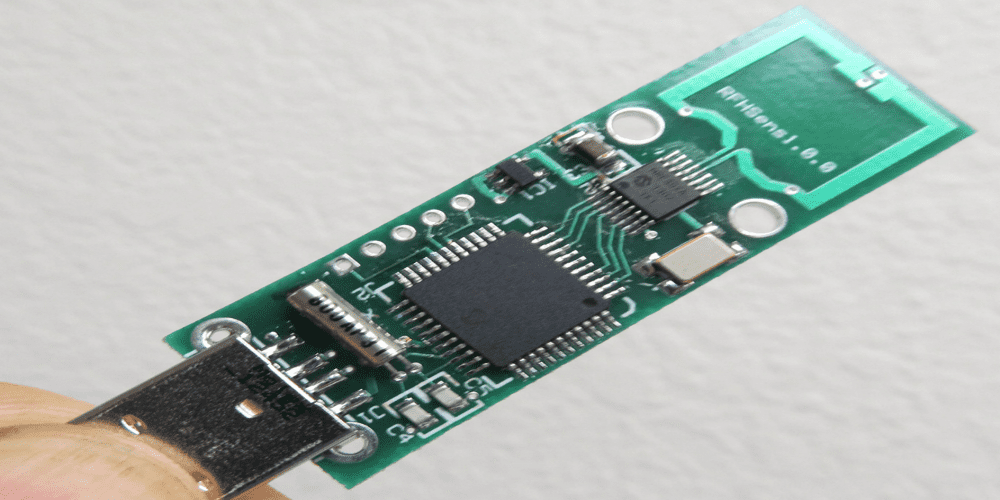
Micro USB PCBs feature a number of key design elements. These elements include surface-mount technology, which allows for smaller and more compact devices. They also feature gold-plated contacts, which provide a reliable and durable connection between the device and the cable. Engineers design these connectors to withstand frequent use and the stresses of daily wear and tear. This approach ensures that the device remains functional and reliable.
One of the key features of micro USB PCBs is their versatility. They are compatible with a wide range of devices, including smartphones, tablets, digital cameras, and portable gaming devices. This versatility allows for the use of a single cable for multiple devices. This versatility aspect makes it a cost-effective and convenient solution for charging and data transfer.
In addition, micro USB PCBs also support fast charging. With this feature you can have a rapid charging of devices in a shorter amount of time. This feature is particularly important for portable devices, which often have limited battery life and require frequent charging.
History and Future of Micro USB PCBs
The Micro USB standard was first introduced in 2007 as a replacement for the Mini USB connector. Manufacturers developed the new standard to address the need for a smaller, more durable, and versatile connector for portable electronic devices, such as smartphones, tablets, and digital cameras. They designed Micro USB PCB to be compatible with the USB 2.0 standard. This approach provided a fast and reliable connection for data transfer and charging.
Over time, Micro USB PCBs have seen several advancements to improve their functionality and performance.
Advancements in Micro USB PCBs
One of the major advancements in Micro USB PCBs is the introduction of SMT. SMT in micro USB PCBs allows for smaller and more compact devices. We can now design lightweight smartphones and tablets that are more portable and easier to use.
Another advancement in Micro USB PCBs has been the development of gold-plated contacts. This advancement provides a reliable and durable connection between the device and the cable. Engineers design these connectors to withstand frequent use and the stresses of daily wear and tear. When there is no wear and tear, the device remains functional and reliable.
Fast charging has also been an important advancement in Micro USB PCBs. With the introduction of Qualcomm’s Quick Charge technology, Micro USB PCBs can now support faster charging speeds. Thus, it reduces the time it takes to charge a device significantly.
The Future of Micro USB PCB
As the demand for efficient electronic devices continues to grow, the future of Micro USB PCBs looks promising. One of the key trends in the electronics industry is the increasing demand for wearable technology, such as smartwatches. Micro USB PCBs are perfect for these devices. This is because they can provide a reliable and durable connection for charging and data transfer.
USB Type-C, which provides faster data transfer speeds may eventually replace the Micro USB PCB as the standard connector. However, Micro USB PCBs will remain in use for several more years due to their compatibility with existing devices.
The Micro USB PCB has undergone several advancements over the years. Researchers have improved its functionality and performance. This is because of the increasing demand for smaller, more efficient, and reliable electronic devices.
Advantages of Micro USB PCBs
1. Smaller Size
The focus of nowadays researchers is to make smaller gadget with more functions. The smaller size of Micro USB PCBs has made them more popular in the electronics industry. The compact size allows for smaller and more portable devices that are easier to carry around. Additionally, it has enabled device manufacturers to create slimmer and lighter devices.

2. Compatibility
Engineers have designed Micro USB PCBs to be compatible with a wide range of devices. This aspect has made them a universal standard for charging and data transfer. This compatibility ensures that users can easily connect and charge their devices. And you don’t have to worry about different cable types or compatibility issues. Additionally, it allows for a seamless transfer of data between devices, regardless of the device type.
3. Ease of Use
The design of Micro USB PCBs is user-friendly, making them easy to use for people of all ages. The connectors have a symmetrical design. It means that you can insert connector either way up. Now the user doesn’t have to fumble with the cable when connecting the devices. Anyone can now connect their devices without any prior technical knowledge.
4. Durability
Manufacturers have designed micro USB PCBs to withstand frequent use, making them durable and long-lasting. They make connectors of high-quality materials that can withstand wear and tear. With this approach the connectors remain functional even after years of use. Additionally, the design of the connectors ensures that they stay firmly in place.
5. Cost-Effective
Micro USB PCBs are cost-effective, making them an ideal option for device manufacturers who are looking to reduce costs. The simple design and wide availability of Micro USB connectors make them a cost-effective solution.
6. Power Efficiency
Micro USB PCBs are power-efficient, allowing devices to conserve power while charging. The connectors deliver power to devices at a steady rate. This is how you can reduce the risk of damage to the battery while ensuring efficient charging.
7. Fast Charging
With the introduction of Qualcomm’s Quick Charge technology, Micro USB PCBs can now support faster charging speeds. This technology reduces the time it takes to charge a device significantly.
8. Easy to Replace
Micro USB PCBs are easy to replace, allowing for quick and simple repairs. This feature has made it easier for users to fix their devices. You don’t have to replace the entire device, saving them time and money.
9. Versatility
Micro USB PCBs are versatile, allowing for a range of applications beyond charging and data transfer. For example, you can use them to power small devices such as LED lights, speakers, and other small electronics.
10. Wide Availability
Micro USB PCBs are widely available. So, they are an easy option for device manufacturers to source. Now consumers can find replacement cables or chargers in case of loss or damage.
The Making of Micro USB PCBs
Micro USB PCBs are an essential component in modern electronic devices. It provides a reliable and efficient connection between electronic devices. In this section you will understand that how manufacturers and designers make these types of PCBs.
· Design
The first step in making a Micro USB PCB is designing the board. This involves using CAD software to create a blueprint of the board. Furthermore, it includes the placement of the Micro USB connector and other electronic components.
· Printing the Board
After finalizing the design, the next step is to print the board. This involves using a special printer to transfer the design onto a copper-coated board. The printer applies a layer of photosensitive material onto the copper surface. Later they transfer the design onto the board using ultraviolet light. The areas of the board with light remain covered with the photosensitive material.
· Etching
After the designer print the board, it undergoes an etching process. This involves immersing the board in a solution that dissolves the exposed copper, leaving only the circuit traces behind. This creates the circuitry that connects the Micro USB connector and other electronic components.
· Drilling and Plating
In this step, engineers drill and plat the board. This involves drilling holes in the board for the electronic components. And then there is plating the board with a layer of metal, typically gold or silver. The plating helps to protect the board from corrosion and provides a stable surface for the components.
· Soldering
The final step in making a Micro USB PCB is soldering the electronic components onto the board. Designers use a machine that places the components onto the board and then solders them into place. Once they solder the components onto the board, it is ready for use in electronic devices.
Conclusion
Micro USB PCBs are an essential component in modern electronic devices. These small and versatile connectors offer many benefits, including quick and easy charging, data transfer, and communication between devices. They are ideal for use in portable devices due to their compact size and durability. The incorporation of Micro USB PCBs has also helped to reduce the overall size and weight of electronic devices.
