Microtek is a leading brand in the power backup industry, known for its reliable and efficient inverters. One of the key components of an inverter is its PCB layout, which plays a crucial role in the overall performance and durability of the device. Microtek has invested heavily in developing high-quality PCB layouts that ensure maximum efficiency and longevity.
The PCB layout of a Microtek inverter is designed to optimize the flow of electrical current, minimize power loss, and prevent overheating. The layout is carefully crafted to ensure that all components are arranged in a way that minimizes interference and maximizes performance. This attention to detail results in an inverter that delivers stable and consistent power output, even under heavy load conditions.
Overview
What is a Microtek Inverter PCB Layout?
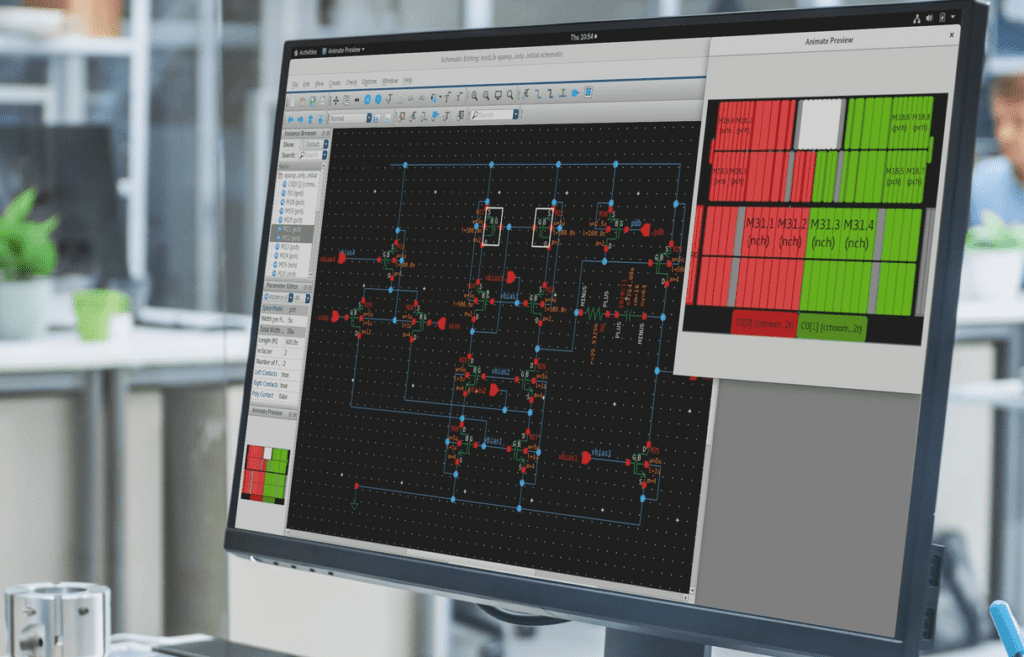
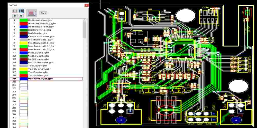
A Microtek inverter PCB layout refers to the design and arrangement of electronic components on a printed circuit board (PCB) used in Microtek inverters. The layout determines how the components are connected and how signals flow through the board.
Why is a Microtek Inverter PCB Layout Important?
The PCB layout plays a crucial role in the performance and reliability of a Microtek inverter. A well-designed layout can ensure efficient power transfer, minimize electromagnetic interference, and reduce the risk of component failure. On the other hand, a poorly designed layout can result in power losses, overheating, or even complete system failure.
In addition, a good PCB layout can make it easier and faster to diagnose and repair faults in the inverter. It can also reduce the manufacturing costs and time required for assembling the inverter.
Overall, a well-designed Microtek inverter PCB layout is critical for ensuring optimal performance, reliability, and cost-effectiveness of the inverter.
Components of a Microtek Inverter PCB Layout
A Microtek inverter PCB layout is a complex system that consists of various components. These components work together to ensure that the inverter operates efficiently and effectively. In this section, we will discuss the four main components of a Microtek inverter PCB layout.
Microcontroller
The microcontroller is the brain of the inverter. It is responsible for controlling and regulating the inverter’s functions. The microcontroller receives signals from the various sensors and switches on the inverter and uses this information to regulate the voltage and frequency of the output waveform. The microcontroller also ensures that the inverter operates within safe limits and shuts down the inverter in case of any malfunctions.
Power Circuitry
The power circuitry consists of the various components that are responsible for converting DC power from the battery into AC power that can be used by appliances. The power circuitry includes components such as transformers, capacitors, and diodes. These components work together to ensure that the output waveform is of high quality and is stable.
Battery Management System
The battery management system is responsible for managing the battery’s charge and discharge cycles. It ensures that the battery is charged efficiently and prevents overcharging, which can damage the battery. The battery management system also monitors the battery’s state of charge and communicates this information to the microcontroller.
Communication Interfaces
The communication interfaces allow the inverter to communicate with external devices such as a computer or a mobile phone. The communication interfaces include components such as USB ports and Bluetooth modules. These components allow the user to monitor the inverter’s performance, change settings, and receive alerts in case of any malfunctions.
In conclusion, a Microtek inverter PCB layout consists of various components that work together to ensure that the inverter operates efficiently and effectively. The microcontroller, power circuitry, battery management system, and communication interfaces are the four main components of a Microtek inverter PCB layout.
Design Considerations

When designing a PCB layout for a microtek inverter, there are several important considerations to keep in mind to ensure optimal performance and reliability. These considerations include the sizing of components, thermal management, and EMI/EMC compliance.
Sizing of Components
The sizing of components is critical to ensure that the inverter operates efficiently and safely. When selecting components, it is important to consider the required voltage and current ratings, as well as the operating temperature range. Choosing components with a higher voltage and current rating than required can lead to unnecessary cost and size, while choosing components with a lower rating can lead to overheating and failure.
Thermal Management
Thermal management is essential to ensure that the inverter operates within a safe temperature range. This can be achieved by selecting components with a low thermal resistance and by designing the PCB layout to minimize heat buildup. Adequate ventilation and heat sinks can also be used to dissipate heat and improve thermal management.
EMI/EMC Compliance
EMI/EMC compliance is important to ensure that the inverter does not interfere with other electronic devices and is not affected by external electromagnetic interference. This can be achieved by using shielding and filtering components, as well as by designing the PCB layout to minimize electromagnetic emissions and susceptibility.
In summary, when designing a PCB layout for a microtek inverter, it is important to consider the sizing of components, thermal management, and EMI/EMC compliance to ensure optimal performance and reliability.
Manufacturing Process
PCB Fabrication
The first step in the manufacturing process of Microtek Inverter PCB layout is the fabrication of PCBs. The PCBs are fabricated using the latest technology and high-quality materials. The process involves the following steps:
- Designing the PCB layout using specialized software.
- Printing the design on a copper-clad board using a laser printer or inkjet printer.
- Etching the copper-clad board to remove the unwanted copper.
- Drilling holes in the board to create the necessary connections.
- Applying a solder mask to protect the copper traces.
Assembly
After the PCBs are fabricated, the next step is to assemble the components on the board. The assembly process involves the following steps:
- Placing the components on the board using automated pick-and-place machines.
- Soldering the components to the board using automated soldering machines or manual soldering.
- Inspecting the board for defects and repairing any defects found.
Testing
Once the assembly is complete, the next step is to test the PCBs to ensure that they are functioning properly. The testing process involves the following steps:
- Powering up the PCB and checking for any shorts or open circuits.
- Testing the voltage and current levels of the PCB.
- Checking the functionality of the PCB by simulating different load conditions.
- Performing a final inspection to ensure that the PCB meets the required standards.
Overall, the manufacturing process of Microtek Inverter PCB layout is a complex and precise process that requires specialized equipment and skilled technicians. The company ensures that each PCB is manufactured to the highest quality standards to ensure the reliability and performance of its products.
Troubleshooting
Common Issues with Microtek Inverter PCB Layouts
Microtek inverters are known for their reliability and durability. However, like any other electronic device, they can experience issues that require troubleshooting. Here are some common issues with Microtek inverter PCB layouts and how to diagnose and resolve them:
-
Inverter not turning on: This is a common issue with Microtek inverters. It can be caused by a faulty battery, loose connections, or a blown fuse. Check the battery voltage and connections to ensure they are secure. If the battery is fine, check the fuse and replace it if necessary.
-
Inverter turning off abruptly: This can be caused by a variety of issues, including overload, short circuit, or overheating. Check the load connected to the inverter and ensure it is within the inverter’s capacity. If the load is fine, check for any loose connections or damaged wires. Also, check the temperature of the inverter and ensure it is not overheating.
-
Inverter producing low output voltage: This can be caused by a faulty transformer, damaged capacitors, or a faulty PCB layout. Check the transformer and capacitors for any visible damage. If they appear fine, check the PCB layout for any loose connections or damaged components.
Diagnosing and Resolving Issues
When diagnosing and resolving issues with Microtek inverter PCB layouts, it is important to follow a systematic approach. Here are the steps to follow:
-
Identify the issue: Determine what the problem is by observing the behavior of the inverter.
-
Gather information: Collect information about the inverter, including its model number, age, and any recent changes made to it.
-
Check the basics: Check the battery voltage, load, and connections to ensure they are all functioning properly.
-
Inspect the PCB layout: Check the PCB layout for any visible damage, loose connections, or damaged components.
-
Test the inverter: Use a multimeter to test the inverter’s output voltage, frequency, and waveform.
-
Replace faulty components: If you have identified a faulty component, replace it with a new one.
By following these steps, you can diagnose and resolve issues with Microtek inverter PCB layouts efficiently and effectively.
