Nur PCB layout is an essential aspect of the printed circuit board design process. It involves the placement and routing of components on the board to ensure optimal performance and functionality. The layout process is crucial in determining the electrical and mechanical characteristics of the PCB.
The design of a PCB layout involves a series of steps, including schematic capture, component placement, and routing. During the schematic capture phase, the designer creates a visual representation of the circuit using software tools. The next step involves placing the components on the board, taking into account factors such as signal integrity, thermal management, and mechanical constraints. Finally, the routing process involves connecting the components with traces while minimizing interference and ensuring signal integrity. A well-designed PCB layout can significantly improve the performance and reliability of electronic devices.
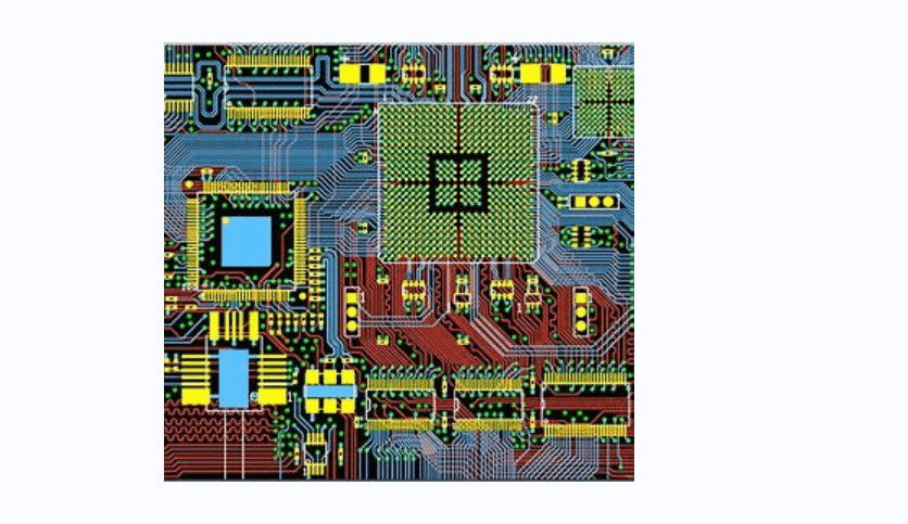
NUR PCB Layout Basics
When designing a PCB layout for NUR (non-uniform rational basis spline) curves, there are a few key principles to keep in mind. NUR curves are widely used in computer graphics and design, and can be a powerful tool for creating complex, organic shapes in PCB layouts.
One important factor to consider when working with NUR curves is the control points. These are the points that define the shape of the curve, and their placement and arrangement can have a significant impact on the final result. It’s important to place control points carefully and thoughtfully, and to adjust their positions as needed to achieve the desired shape.
Another consideration is the degree of the curve. This refers to the number of control points used to define the curve, and can have a big impact on the smoothness and complexity of the resulting shape. Higher-degree curves can be more complex and difficult to work with, but can also offer more flexibility and precision in the final design.
When working with NUR curves in PCB layouts, it can be helpful to use specialized software or tools that are designed to handle these types of curves. This can help to streamline the design process and ensure that the final layout is accurate and well-optimized.
Overall, understanding the basics of NUR PCB layout is an important part of designing complex, organic shapes in PCB design. By carefully considering control points, degree, and other key factors, designers can create layouts that are both functional and visually appealing.
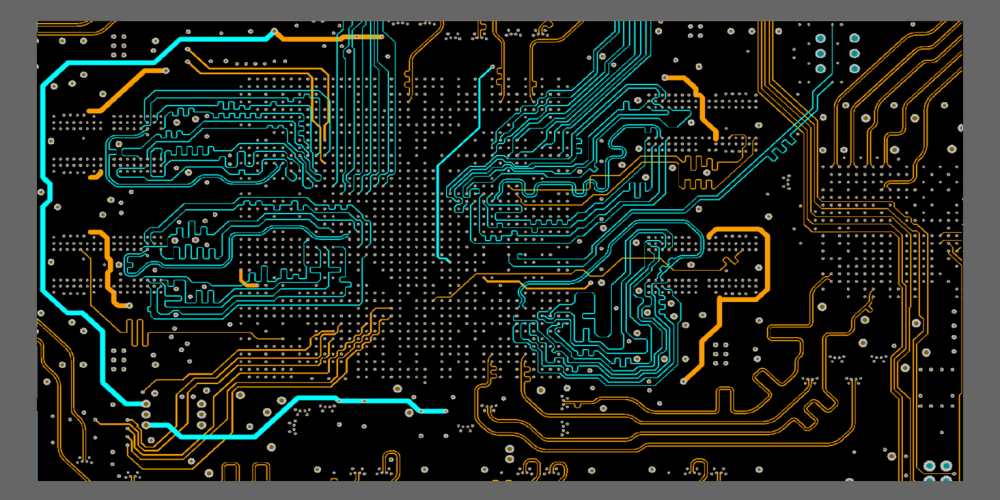
NUR PCB Layout Process
The NUR PCB Layout Process is a systematic approach to designing printed circuit boards that are optimized for performance and manufacturability. This process involves several key steps, including:
-
Schematic Design: The first step in the NUR PCB Layout Process is to create a schematic diagram of the circuit. This diagram shows the connections between components and helps to ensure that the circuit is properly designed.
-
Component Placement: Once the schematic is complete, the next step is to place the components on the PCB. This involves determining the optimal placement of each component to minimize noise, improve signal integrity, and ensure that the board can be manufactured efficiently.
-
Routing: After the components are placed, the next step is to route the traces on the PCB. This involves determining the optimal routing paths for each trace to minimize noise and interference, and to ensure that the board can be manufactured efficiently.
-
Design Rule Checking: Before the PCB design is finalized, it is important to perform a design rule check to ensure that the design meets the requirements of the manufacturer. This involves checking for errors such as trace width violations, clearance violations, and other issues that could impact the manufacturability of the board.
-
Gerber File Generation: Once the design is complete and has been verified, the final step is to generate the Gerber files that will be used to manufacture the board. These files contain all of the information needed to produce the PCB, including the placement of components, the routing of traces, and other important details.
By following the NUR PCB Layout Process, designers can create printed circuit boards that are optimized for performance, reliability, and manufacturability. This process helps to ensure that the design meets the requirements of the manufacturer, and that the board can be produced efficiently and cost-effectively.
NUR PCB Layout Software

NUR PCB Layout Software is a powerful tool for designing printed circuit boards. It is a user-friendly software that allows users to create and edit PCB designs quickly and efficiently. The software is designed to work with a wide range of PCB design requirements, from simple single-layer designs to complex multi-layer designs.
One of the key features of NUR PCB Layout Software is its intuitive interface. The software provides a range of tools and features that are easy to use, even for those who are new to PCB design. The software also includes a range of templates and pre-designed components, making it easy to get started on a new design.
Another key feature of NUR PCB Layout Software is its ability to handle complex designs. The software includes advanced routing algorithms that can handle even the most complex PCB designs. It also includes a range of design rules that can be customized to meet specific design requirements.
NUR PCB Layout Software also includes a range of collaboration tools that make it easy to work with other members of a design team. The software allows users to share designs and collaborate in real-time, making it easy to work on designs together.
Overall, NUR PCB Layout Software is a powerful and user-friendly tool for designing printed circuit boards. Its intuitive interface, advanced routing algorithms, and collaboration tools make it a great choice for both novice and experienced PCB designers.
NUR PCB Layout Best Practices
When designing a PCB layout for NUR applications, it is essential to follow some best practices to ensure that the circuit functions correctly. Here are some of the best practices that you should consider:
Component Placement
The placement of components on the PCB is crucial to ensure that the circuit works correctly. You should place components in a way that minimizes the length of the traces between them. This will reduce the chances of signal interference and noise.
Signal Traces
Signal traces should be kept as short as possible to minimize the chances of signal interference and noise. You should also ensure that the traces are wide enough to carry the required current without overheating.
Ground Plane
A ground plane is essential in NUR PCB layout to reduce the chances of electromagnetic interference (EMI). You should ensure that the ground plane is continuous and has a low impedance path to the power source.
Power Planes
Power planes should be used to provide a low impedance path for power to flow through the circuit. You should ensure that the power planes are placed adjacent to the ground plane to reduce the chances of EMI.
Routing
When routing traces, you should ensure that they do not cross over each other. This will reduce the chances of signal interference and noise. You should also use 45-degree angles when routing traces to reduce the chances of reflections.
Thermal Management
Thermal management is crucial in NUR PCB layout to ensure that the circuit does not overheat. You should ensure that the PCB has enough copper to dissipate heat and that components are placed in a way that allows for proper airflow.
By following these best practices, you can design a NUR PCB layout that functions correctly and reliably.
NUR PCB Layout Troubleshooting
When designing a PCB layout for a NUR (Non-Uniform Rational B-Spline) system, there are several common issues that may arise. Troubleshooting these issues requires a systematic approach and a thorough understanding of the NUR system. Here are some common problems and their solutions:
Issue: Poor Signal Quality
One of the most common issues with NUR PCB layouts is poor signal quality. This can be caused by a variety of factors, including improper layout, poor grounding, and electromagnetic interference (EMI).
To troubleshoot this issue, start by checking the layout. Make sure that the traces are properly routed and spaced, and that there are no crossovers or sharp turns. Next, check the grounding. Make sure that the ground plane is properly connected and that there are no ground loops. Finally, check for EMI. This can be caused by nearby power sources, other PCBs, or even nearby electronic devices. Use shielding or filters to reduce EMI.
Issue: Inconsistent Performance
Another common issue with NUR PCB layouts is inconsistent performance. This can be caused by a variety of factors, including improper component placement, poor soldering, and temperature variations.
To troubleshoot this issue, start by checking the component placement. Make sure that all components are properly placed and oriented. Next, check the soldering. Make sure that all connections are properly soldered and that there are no cold joints or solder bridges. Finally, check for temperature variations. This can be caused by nearby heat sources or changes in ambient temperature. Use thermal management techniques to reduce temperature variations.
Issue: Crosstalk
Crosstalk is another common issue with NUR PCB layouts. This occurs when signals on adjacent traces interfere with each other, causing signal degradation or noise.
To troubleshoot this issue, start by checking the layout. Make sure that the traces are properly spaced and that there are no crossovers. Next, use shielding or filters to reduce crosstalk. Finally, consider using differential signaling to further reduce crosstalk.
In conclusion, troubleshooting NUR PCB layouts requires a systematic approach and a thorough understanding of the NUR system. By identifying common issues and their solutions, you can ensure that your NUR system performs optimally.
