To those who have never ordered PCBs before, the process can seem difficult. Most of this can get handled by your engineer if you choose to outsource your electronics design; however, if you’re planning on handling this on your own. You’ll quickly learn that there are many intricate details and requirements to master.
In any case, as the company’s creator, you should know at least the very minimum about what’s needed to order replacement circuit boards.
To help you weigh the pros and cons of each option, I’ll explain all of the technical details in this article. Although the precise terminology for a few of these requirements may differ from one manufacturer to the next, the specs themselves will be universally applicable no matter where you choose to have your boards made.
Basics to Order Custom PCB
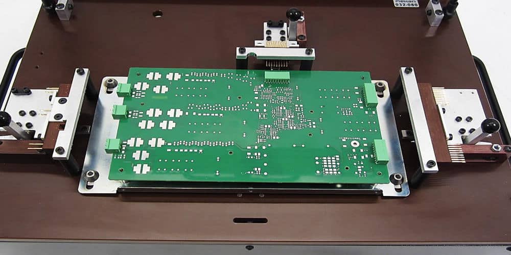
An assembled printed circuit board is the result of two primary processes. First, the creation of the bare board. And second, the soldering of each of the parts. All the different requirements get broken down into these two main categories for easier comprehension.
In order to have your printed circuit board fabrication ordered. You will have to provide the supplier with files known as Gerbers.
A Bill of Materials detailing the PCB assembly’s constituent parts is necessary, as is Pick-and-Place data detailing the components’ precise placements for use in automating the soldering process. PCB designing software also creates these two files.
1. Type of Board:
Pick “single pieces” almost always. The fabrication of PCBs does not occur on a one-to-one basis. Instead, many duplicates of your board will get manufactured on a single panel. Therefore, the fabrication of smaller boards can get streamlined.
Depanelization refers to the process of separating the constituent electronic boards on each panel. After PCB fabrication or even after the final inspection has been finished.
The majority of the time, manufacturers will ship you fully completed and partitioned circuit boards, relieving you of the burden of penalization.
2. Different Panel Design:
In some cases, a single panel may house multiple boards. You can reduce production costs by having all of the necessary boards for your product mounted on the same panel. However, there is a cost associated with having panels with many board variations.
3. Size:
You should expect to pay more per square inch for a PCB with these dimensions. So keep that in mind if you’re only ordering a few. These are the panel measurements for ordering purposes.
4. Quantity (Single):
The minimum number of boards for the first prototype should be five, and as your faith in the concept grows, you can add more.
5. Layers:
Your PCB design employs this many routing layers. Every number of layers beyond the first is an even number. A basic printed circuit board (PCB) often has only one or two layers. These are the bottom and top layers. Designs with a moderate level of complexity (such as microcontrollers) typically have four to six layers. Whereas designs with a higher level of complexity (such as microprocessors) typically have eight layers or more. The PCB’s price is proportional to its number of layers.
6. Material:

Between the several layers of routing material on a printed circuit board, the is the foundational material. FR-4 is widely available and suitable for most designs.
Due to the high price of incorporating blind and buried vias onto a circuit board, they are often reserved for situations when space constraints are absolutely essential. Because normal vias are through holes, they traverse every layer, even those that don’t require them. The layers in which the vias are not connected can be a waste of space. A blind via is a connection from outside layers to inner layers that only has one end that is visible on the finished board. Instead of using a through the hole, the final board uses a hidden via to connect the innermost layers.
7. Thickness:
At this point, the board has reached its full thickness. 1.6 millimeters (0.062 inches) is the standard thickness. If you need to save room or cut down on weight, use a board with a slimmer profile. A thicker board is preferable if the durability of the electronic board is essential.
8. Minimum Spacing / Track:
This is the smallest width that can get used for routing tracks or traces, as well as the smallest distance that can get left between traces. Mils are the units used for this. A mil is a 1000th part of an inch. The typical thickness is six mils, although in cases when space is at a premium, three to five mils may be required. The price jumps up dramatically if you drop below 6 millimeters.
9. Minimum hole size:
What this means is that this is the smallest hole that can be bored. This is the standard size for the hole used in vias to interconnect traces between layers. Since vias typically require a lot of room, having smaller hole sizes will allow for denser packing of the elements.
10. Soldering Mask:
The purpose of the solder mask is to prevent solder bridges and oxidation between neighboring solder pads. This becomes possible by acting as a protective covering on the outside layers of the board. Green is the default option, but you can choose from a variety of different colors if you want.
11. Silkscreen:
Simple graphics (logo) and text can be added to your board using the silkscreen layer. In most cases, it will append the identities of the individual parts.
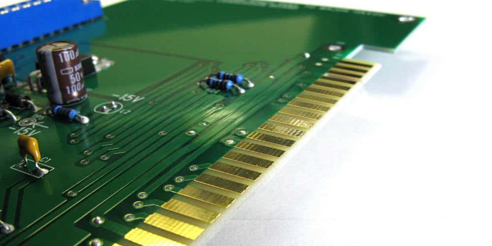
If your board uses edge connections, you should have its gold plated to prevent corrosion and wear and tear.
12. Gold Fingers:
Edge connectors on your board should be gold-plated to prevent corrosion and damage.
13. Surface Finish:
The surface finish serves to protect the board’s uncovered copper pads from corrosion and increase its solderability by providing a coating. Lead-based HASL was once the standard, but lead-free ENIG has now taken its place. The use of Ag, immersion silver, is another method of plating that does not include lead.
14. Via Procedure:
Though open vias are the norm, there are instances where they must be sealed. Tenting the via, or letting the soldering mask layer cover it up, is the cheapest and easiest approach. Because there is no need for an additional cost. The tenting method is more effective for vias with a narrower diameter.
Filling or plugging the vias is a more expensive technique. When placing vias in close proximity to the chip pins, as is necessary for tightly spaced BGA packaging, this technique is frequently employed. These vias can result in a bad soldering connection between the chip pin and the board. In this situation, plugging the vias should do the trick.
15. Finished weight of copper:
Over one sq. ft, this is how much the copper layer weighs. The thickness of the copper is actually being measured. One ounce of copper is equivalent to about 1.4 mils. In high-power systems, when a smaller trace width is needed to transport the same level of current, thicker traces of copper are typically employed. The next several tiers of the network’s routing structure will use this.
16. Inner copper weight:
For the total copper weight of the completed product, see above. This is the weight of copper for the interior routing layers. It is generally recommended that high-current traces be routed on the board’s outer layers, where heat may be dissipated more efficiently.
Conclusion
RayPCB and Hillmancurtis in China are two of our preferences, especially when we need to buy professionally made boards. Whether in small batches for prototyping or in larger batches for production.
Boards can be assembled by hand, but unless you’re an expert solderer, we wouldn’t advise doing so. The vast majority of today’s microchips are too small to get soldered by hand.
Another major drawback of hand soldering is the difficulty in determining if problems with the design are the result of poor soldering or other, more basic design flaws. Have a professional producer produce your boards and assemble your product. It will make testing and debugging your idea a simple task.
