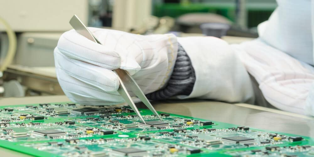
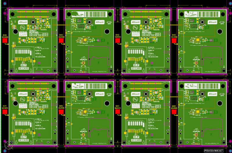
Panelization is a process that involves placing multiple PCB designs onto a single panel. This technique is used to produce multiple PCBs simultaneously, reducing manufacturing costs and improving efficiency. Altium is a popular software tool used for designing and panelizing PCBs.
Panelization offers several benefits over traditional PCB manufacturing methods. By placing multiple PCB designs onto a single panel, manufacturers can reduce the amount of material waste and increase production efficiency. Additionally, panelization can help to reduce the cost of manufacturing PCBs, making it a popular choice for companies looking to streamline their production processes. With the help of Altium, designers can easily create and optimize panelized PCB designs, ensuring that they meet the unique needs of their clients.
What is Panelization in Altium?
Benefits of Panelization
Panelization is the process of arranging multiple PCB designs into a single panel for manufacturing. This technique offers several benefits, such as:
- Cost savings: Panelizing PCBs can reduce the cost of manufacturing, as it allows for more efficient use of materials and equipment.
- Improved yield: Panelization can help improve yield rates, as it allows for better control over the manufacturing process.
- Faster production: By panelizing multiple PCB designs, manufacturers can save time and reduce lead times for customers.
Types of Panelization
There are several types of panelization, including:
- Single PCB panelization: This involves arranging multiple copies of the same PCB design onto a single panel.
- Mixed PCB panelization: This involves arranging multiple different PCB designs onto a single panel.
- Step-and-repeat panelization: This involves repeating the same PCB design multiple times on a single panel, with each instance rotated or mirrored.
Steps to Panelize a Design
To panelize a design in Altium, follow these steps:
- Open the PCB design you want to panelize.
- Click on the “Design” menu and select “Panelize.”
- Choose the panel size and layout you want to use.
- Drag and drop the PCB designs you want to include onto the panel.
- Arrange the designs as desired and add any necessary fiducials or tooling holes.
- Export the panelized design files for manufacturing.
By following these steps, you can easily panelize your PCB designs in Altium and take advantage of the benefits that this technique offers.
Design Considerations for Panelization
When designing a printed circuit board (PCB) for panelization, there are several key design considerations that must be taken into account. These considerations include component placement, routing, and manufacturing constraints.
Component Placement
When designing for panelization, it is important to consider the placement of components on the PCB. Components should be placed in a way that allows for easy assembly and disassembly of the panelized PCBs. This means that components should be placed in a way that allows for easy access to the panel edges, where the PCBs will be separated from the panel.
Routing
Routing is another important consideration when designing for panelization. The routing of the PCB should be done in a way that allows for easy separation of the panelized PCBs. This means that traces should be routed in a way that avoids the edges of the panel, where the PCBs will be separated.
Manufacturing Constraints
Manufacturing constraints are also an important consideration when designing for panelization. The panelized PCBs must be designed in a way that is manufacturable within the constraints of the manufacturing process. This means that the panelized PCBs must be designed in a way that allows for easy assembly and disassembly, and that the panelized PCBs must be designed in a way that is compatible with the manufacturing process.
In conclusion, when designing for panelization, it is important to consider component placement, routing, and manufacturing constraints. By taking these considerations into account, designers can ensure that their panelized PCBs are easy to assemble and disassemble, and that they are compatible with the manufacturing process.
Panelization Techniques

When it comes to designing printed circuit boards (PCBs), panelization is a crucial step in the manufacturing process. Panelization is the process of arranging multiple PCBs onto a single larger board, known as a panel. This technique helps to optimize the manufacturing process by allowing multiple PCBs to be fabricated simultaneously.
In Altium, there are several panelization techniques available to designers. In this section, we will explore three of the most common techniques: Tab Routing, V-Score, and Depanelization.
Tab Routing
Tab routing is a technique in which the individual PCBs are held together by small tabs of material that are left intact during the manufacturing process. These tabs can be easily broken off after the PCBs are assembled. Tab routing is a popular technique because it is relatively simple to implement and it allows for easy separation of the individual PCBs.
V-Score
V-Score is another popular panelization technique that involves creating a groove or score line in the panel material. This groove allows the individual PCBs to be easily separated after the manufacturing process is complete. V-Score is a versatile technique that can be used with a variety of materials, including FR4, aluminum, and stainless steel.
Depanelization
Depanelization is a more complex panelization technique that involves cutting or routing the individual PCBs out of the panel material. This technique requires specialized equipment and expertise, but it can be useful in situations where other panelization techniques are not suitable. Depanelization is often used when the PCBs are irregularly shaped or when the panel material is too thick for tab routing or V-Score.
In conclusion, panelization is an essential step in the PCB manufacturing process, and Altium offers a variety of panelization techniques to suit different design requirements. Whether you choose tab routing, V-Score, or depanelization, it is important to carefully consider the needs of your design and choose the technique that best meets those needs.
Panelization Best Practices
Panelization Tool Selection
When selecting a panelization tool, it’s important to consider the specific requirements of your project. Altium offers a variety of panelization tools that can be used to optimize your design for manufacturing. Some of the key factors to consider when selecting a panelization tool include:
- Compatibility with your design software
- Ease of use and flexibility
- Ability to generate accurate manufacturing data
- Compatibility with your manufacturing process
Panelization Workflow
The panelization workflow can be broken down into several key steps:
- Importing the design files into the panelization tool
- Defining the panel layout and adding tooling holes
- Adding fiducial marks and other manufacturing data
- Generating the manufacturing data and exporting the panel design
It’s important to follow a consistent and well-defined panelization workflow to ensure that your design is optimized for manufacturing and meets the requirements of your specific manufacturing process.
Design for Manufacturing
When designing for panelization, there are several key considerations to keep in mind:
- Component placement: Components should be placed with sufficient clearance to allow for tooling holes and fiducial marks.
- Trace routing: Trace routing should take into account the location of tooling holes and fiducial marks, and should be optimized for the specific manufacturing process.
- Panel layout: The panel layout should be optimized for the specific manufacturing process, taking into account factors such as panel size, material thickness, and tooling hole placement.
By following these best practices for panelization, you can ensure that your design is optimized for manufacturing and meets the requirements of your specific manufacturing process.
