Now, you’ve completed a perfect design for your PCB. Next, you laid your traces and components out carefully to ensure optimal thermal and EMI/EMC considerations. Also, you’ve done a great job ensuring that your board is perfectly fitted within the end product’s tight enclosure.
Now, you discover there’s an issue. Your usual fabrication house reveals to you that their transfer conveyors will not be able to process any single board having a conveyor width below 2.0 inch. Once you want your business to move forward, your sales liaison may likely advise you to try panelization or make it larger or bigger.
The enclosure of your product design lacks the required margin to get your board’s width expanded. Even though this is possible, the price required for the processing of a single board looks a bit steep. This is where PCB panelization comes in.
In this article, we will be considering what PCB panelization is, what pc b panel is, panel circuit board, pcb panelization tool, Altium panelization and KiCad panelization. Please continue reading to learn more.
What is a PCB Panel?
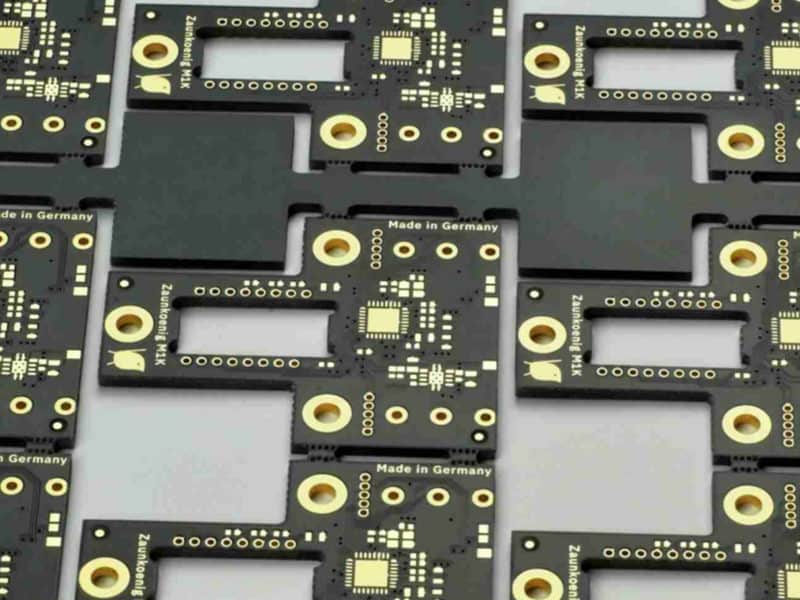
A PCB panel results after combining some PCB unit boards together. This is possible using different possible modes of connection.
Anytime hardware designers design a printed circuit board, they consider the component’s layout and electrical signal present on the panel circuit board. This is done to focus on the product’s function. Less attention is paid to the production and assembly of the PCB. To ensure the production of the PCB comes out smooth, most especially during the SMT assembly.
To ensure that the entire PCB production holds smoothly, make sure you give special attention to the design of your PCB assembly.
Request PCB Panelization Services, Pls Send PCB Files to Sales@raypcb.com Now
The Significance and Purpose of the PCB Panel
Improves efficiency of the SMT assembly
The more the number of PCB unit boards contained in a panel, the lesser the time required for one PCB to run in orbit and transfer. This also leads to a higher rate of utilization of the pasting equipment. This can improve the SMT’s production efficiency greatly.
Improves the SMT production quality to prevent any bad issue during the process of production
The distribution density of the PCB components is big. Some components like edge connectors outline could be beyond the printed circuit board’s edge.
Prevents damage and it can be operated with ease
The design of the PCB panel is done to facilitate the production line’s operation. A PCB assembly has to pass through so many steps. Your semi-finished PCB or finished PCB should be placed into your turnover box. These PCBs will further be transferred, kept, and also transported through the turnover rack. To carry out these operations, there’s a need for a unique process edge. This helps in preventing damage from coming to the components present on the board of the PCB.
Types for the Panel Design
Now, no matter the PCB type, there’s a need to utilize a panel structure. Moreover, designing panels comes in various ways. At times, it may be difficult to tell the best way or manner to use it, as well as the number or amount of panels required.
The manufacturing of PCB panels can be done in different ways. These include AAAA, ABCD, or ABAB. Generalizing which panel type is good isn’t easy. This is determined by taking a look at the distribution and density of the board’s components, coupled with the equipment’s configuration.
PCB Panelization: What is this?
PCB panelization has to do with a technique for manufacturing, where smaller boards are produced in large quantities and also joined together as just one array. This makes it very easy to move via an assembly line.
These boards can be removed or depanelized easily from this array for the installation or packaging into a specific product. In addition, having a processing edge around the board helps in increasing its width. This helps it fit perfectly on its assembly line.
To enjoy the advantages gained from mass production as a result of panelization, there’s a need to make use of these design considerations.
Strength of the PCB-array
Between the array integrity and depanelization ease during production, there exists a tradeoff. Vibration can be reduced and the strength can be increased when the board count for each array is increased.
The layout of the component
The placement of the connectors and components, most especially those that hang off the board’s edge may limit your options for panelization. Take note of the sensitive surface mount technology (SMT) component’s location towards a board’s edge.
Tooling holes
Breakaway processing edges and arrays can provide you with the required space for holes tooling for automatic testing.
The shape of the PCB
Your board’s shape can complicate your panelization. It is okay to work with rectangles. However, if your board’s shape is complex, then you can maximize a panel’s shape by alternating the images from 90 degrees to 180 degrees. Utilize a CAD program n fitting boards that are unusually shaped into an array.
Benefits of PCB Panelization
Doing PCB panelization will not just assist the smaller boards to fit in the standard processes of production, it also ensures more efficient production. Let’s consider the common benefits you enjoy from PCB panelization.
Mass production: To build many boards, PCB panelization is best. This is because it will help save you money and time.
Safety of the product: With panelization, your PCB will be protected from vibration and shock which usually occurs during assembly.
Efficiency and speed: During the processes involved, i.e. paste printing, the assembly of the component, soldering, and testing, you will need things to be done more efficiently and faster to help in processing multiple boards all at once.
Standard sizes of the panel: Most times, it is very cost effective when using the standard panel of the fabricator for producing boards.
Every producer has their personal preferences when it comes to sizes of panels. However, generally, the standard is panels of 18 by 24 inch with a half inch clearance perimeter to handle boards with double sides. For multilayer boards, use 1 inch. Make sure you get some information from your fabricator before you draft a panel for the assembly process.
Request PCB Panelization Services, Pls Send PCB Files to Sales@raypcb.com Now
Methods of Depanelization
The depanelization of the array of boards that are smaller comes in many ways. Whichever way you use usually depends on the manner in which you connect these boards together in your panel.
Tabs
You can connect individual circuits to your panel frame through narrow tabs. This can be broken or snapped to get rid of the boards. You can subject it to some automated or manual processes.
V-grooves
This is also referred to as v-scoring. V-grooves deal with the tracing of a v-shaped cut passing through the panel’s bottom and top edge. Typically, boards are usually scored to around one-third of the thickness. You must use a machine or fixture in depaneling it. This is because removing it manually can place some strain on the components located near the edge.
Below are the methods for depanelization
Die cutting/punch: Fixtures having die cutters are utilized in punching the individual boards from a panel. Also, the blades and fixture have to be customized to work with the board.
Manual: Go back to the plastic model robots, planes, and cars you built back then when you were a kid? You can cut the boards or pop them out of a channel using a fixture, tool, or using your hand. However, this step requiring intensive labor is usually phased out as a result of concerns relating to quality, as well as the rise.
Depaneling router: Just like the wood router, the machine features a bit, which can be utilized in cutting off boards from your panel.
Saw cut: You can line up a saw blade with v-groove. After this, you can use it in cutting the boards from the panel.
Laser cut: At times, this is referred to as a laser router. Normally, lasers are great for designs having unusual shapes or tight tolerances. This process is totally automated, and can be utilized in carving paths that include sharp corners and curves. Also, it doesn’t cause mechanical stress.
Why PCB Panelization is Important
Asides performance, compliance with the standard requirements, and functionality, there’s a need to include manufacturability as a factor into the designs of your printed circuit boards. Designing boards having panelization on your mind will help in preventing redesigns and delays that are unplanned.
PCB Panelization Tools
There are several PCB panelization tools available. The two main tools for PCB panelization is altium designer and KiCad. Let’s discuss them further.
Altium Panelization
Altium Designer is one of the best software for PCB panelization. Circuit boards are available in different sizes and shapes. PCB manufacturers must be careful to carry out PCB Panelization carefully. Altium panelization tools are specifically designed to carry out your panelization tasks effectively. This software includes a lot of features for panelization. Here, we will discuss how to perform altium panelization.
You need to decide the size and shape of your PCB before getting started with Altium designer. After that, your blank PCB should be ready as you will be working with it in your layout. You will have to visit File, then click New, and choose PCB. You will have to give your project a name. Then, you have created the PCB. You can now commence work on your board outline.
How to Create a Simple Board Outline with Altium
The default PCB size for a rectangular PCB outline in Altium Designer is 6 inches by 4 inches. The board outline can be used and modified according to the specified requirements.
To achieve this, you will have to set the origin. Go to Edit, click Origin, and choose Set. Click on your mouse to set the origin.
The next step is to set your grid. Visit the grid manager in the board’s properties menu. You can also press CTRL +Shift + G to set the grid. There are other useful functions available in the grid manager.
Altium designer features three modes for its design process. The modes are the 2D layout mode, the board planning mode, and the 3D layout mode. The board planning mode is the right mode for working with your board outline.
KiCad Panelization
KiCad panelization is not as difficult as you think. A new script (python-based) exists which helps in panelizing KiCad circuit boards. Jan Mrazek is in charge of this project referred to as KiKit and functions well on the .kicad_pcb files, and helps in arranging them on a grid, with the v-cuts or mousebites you prefer. This is necessary for board’s separation when the production of the boards is complete.
When you work with a smaller board, the common practice is grouping them together into panels. By doing so, you are speeding up the assembly of the printed circuit board. This is because multiple boards may have the application of the solder paste, pass through the pick and place machine, and then sent as one unit to the reflow oven.
This is usually done manually. However, most of the time this script saves you much time while giving you the desired results. Using this KiKit, it is possible to gang up about six boards at once, making use of mousebites in keeping them all together all through the production process. However, it still ensures easy separation when you’ve soldered all its components.
Conclusion
After reading through this guide, you will have learnt much about PCB panelization and why it is so important. We also discussed PCB panels in detail. PCB panelization is a very important tool when talking about ensuring efficiency during the manufacturing of printed circuit boards. Asides improving the efficiency of production it also reduces the time for delivery, and can solve countless logistic issues by utilizing PCB panels the right way. If you feel you wish to learn more or have any questions, feel free to ask us. We are always here for you!
