Printed Circuit Board (PCB) layout is an essential aspect of electronics design, as it plays a crucial role in ensuring the functionality and reliability of electronic devices. PCB layout involves arranging electronic components and interconnecting traces on a board to create a functional circuit. The layout process is critical, as it directly impacts the performance, cost, and manufacturability of the final product.
The PCB layout process involves a series of steps, including schematic capture, component placement, and routing. During schematic capture, the circuit is designed using a software tool that allows the designer to create a virtual representation of the circuit. Once the schematic is complete, the designer moves on to component placement, where the components are arranged on the board to optimize performance and minimize size. Finally, routing involves connecting the components with traces on the board, which can be done manually or using automated routing tools.
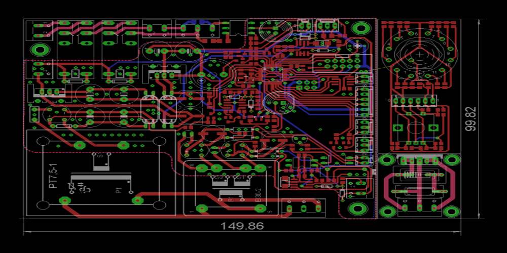
Basics of PCB Circuit Layout
Components Placement
One of the most critical aspects of PCB circuit layout is component placement. The placement of components on a PCB can affect the performance and reliability of the circuit. It is essential to place components in a way that allows for efficient routing of traces while avoiding interference and crosstalk.
When placing components on a PCB, it is crucial to follow the manufacturer’s recommendations for spacing and orientation. Components should be placed in a logical and organized manner, with similar components grouped together.
Routing
Routing refers to the process of connecting the components on a PCB using copper traces. The routing of a PCB can significantly impact the performance and reliability of the circuit. It is essential to keep the routing as short and direct as possible to minimize signal loss and interference.
When routing a PCB, it is crucial to follow the design rules specified by the manufacturer. These rules define the minimum trace width and spacing, as well as the maximum number of vias that can be used.
In addition to following the design rules, it is essential to consider the placement of components when routing a PCB. Components that are closely spaced should be connected with short traces to minimize interference and crosstalk.
Overall, the basics of PCB circuit layout involve careful consideration of component placement and routing. By following the manufacturer’s recommendations and design rules, it is possible to create a reliable and efficient circuit.
Considerations for PCB Circuit Layout
Signal Integrity
When designing a PCB layout, signal integrity is a crucial consideration. Signal integrity issues can cause noise, distortion, and other problems that can affect the performance of the circuit. To ensure good signal integrity, it is important to consider the following:
- Trace routing: Keep traces as short and direct as possible to minimize signal loss and interference.
- Ground and power planes: Use ground and power planes to provide a low-impedance path for signals and reduce electromagnetic interference (EMI).
- Component placement: Place components carefully to minimize the distance between them and reduce the length of traces.
Power Integrity
Power integrity is another important consideration when designing a PCB layout. Power integrity issues can cause voltage fluctuations, noise, and other problems that can affect the performance of the circuit. To ensure good power integrity, it is important to consider the following:
- Decoupling capacitors: Use decoupling capacitors to filter out high-frequency noise and ensure a stable power supply.
- Power plane placement: Place power planes close to ground planes to reduce the impedance of the power supply path.
- Trace width: Use wider traces for high-current paths to reduce resistance and voltage drop.
Thermal Management
Thermal management is also an important consideration when designing a PCB layout. Overheating can cause components to fail and affect the performance of the circuit. To ensure good thermal management, it is important to consider the following:
- Component placement: Place components to allow for adequate airflow and heat dissipation.
- Heat sinks: Use heat sinks to dissipate heat from high-power components.
- Trace width: Use wider traces for high-current paths to reduce resistance and minimize heat generation.
By considering these factors, designers can create PCB layouts that have good signal integrity, power integrity, and thermal management.
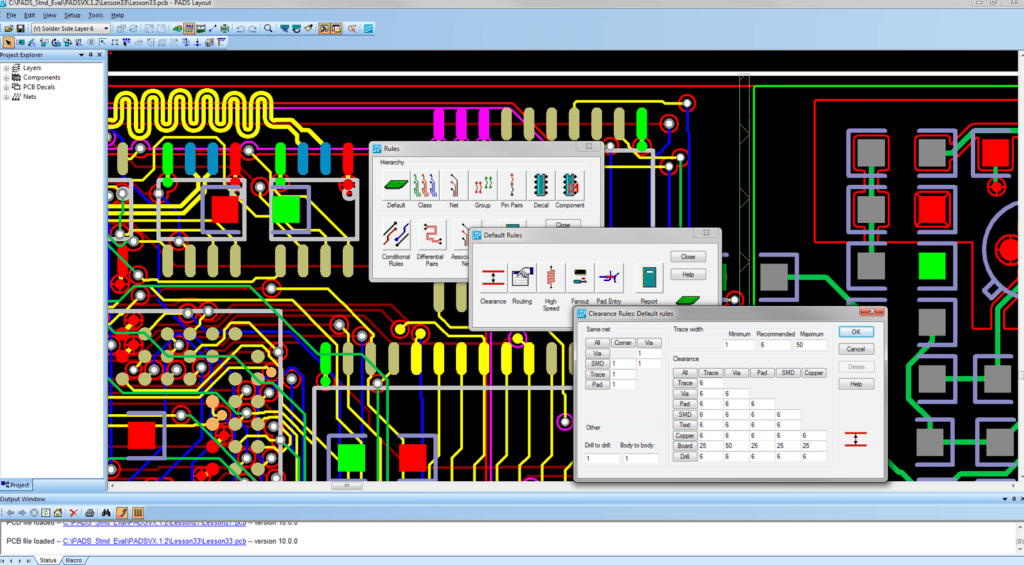
Tools for PCB Circuit Layout

When it comes to PCB circuit layout, there are several tools that can help you create a successful design. These tools can assist with everything from designing the schematic to simulating the circuit to manufacturing the final product. Here are the three main types of tools for PCB circuit layout:
PCB Design Software
PCB design software is a crucial tool for creating a PCB circuit layout. This software allows you to create a schematic of your circuit and then design the physical layout of the PCB. Some popular PCB design software options include Altium Designer, Eagle PCB, and KiCAD. These programs offer a wide range of features, including the ability to create custom components, generate Gerber files, and perform design rule checks.
Simulation Tools
Simulation tools allow you to test your circuit design before you manufacture the PCB. These tools can help you identify potential issues with your design and make any necessary changes before you move forward with production. LTSpice and Proteus are two popular simulation tools that offer a variety of features, including the ability to simulate analog and digital circuits, perform Monte Carlo analysis, and generate output waveforms.
Manufacturing Tools
Once your PCB design is complete, you’ll need to manufacture the final product. Manufacturing tools can help you create a high-quality PCB that meets your specifications. Some popular manufacturing tools include PCB milling machines, soldering stations, and pick-and-place machines. These tools can help you create a professional-looking PCB that works as intended.
In conclusion, using the right tools is essential for creating a successful PCB circuit layout. PCB design software, simulation tools, and manufacturing tools can all help you create a high-quality design that meets your needs. By taking advantage of these tools, you can save time, reduce costs, and ensure that your PCB works as intended.
Best Practices for PCB Circuit Layout
Design for Manufacturability
When designing a PCB circuit layout, it’s essential to keep manufacturability in mind. Here are some best practices to follow:
- Keep the board size and shape as simple as possible to reduce costs.
- Place components on one side of the board to reduce assembly time and costs.
- Use standard board sizes and hole sizes to reduce tooling costs.
- Keep the trace width and spacing within the manufacturer’s capabilities to ensure high yields.
Design for Testability
Designing a PCB for testability is crucial to ensure that the board functions correctly. Here are some best practices to follow:
- Include test points on the board to enable easy access for testing.
- Use boundary scan testing to test the board’s connectivity and functionality.
- Use built-in self-test (BIST) circuits to test the board’s functionality automatically.
- Use in-circuit testing (ICT) to test the board’s components.
Design for Assembly
Designing a PCB for assembly is essential to ensure that the board can be assembled correctly and efficiently. Here are some best practices to follow:
- Place components in a logical and organized manner to reduce assembly time.
- Group components that are frequently assembled together to reduce handling time.
- Use surface mount technology (SMT) components to reduce assembly time and costs.
- Use automated assembly equipment to reduce assembly time and costs.
Following these best practices will help ensure that your PCB circuit layout is manufacturable, testable, and easy to assemble, resulting in a high-quality, reliable board.
