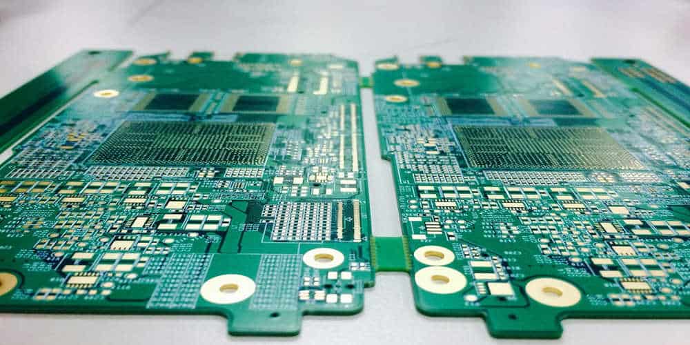
A PCB is a small board of green color with lines on it that resembles a maze and may get found inside many different types of electronic equipment.
In other words, what exactly is a printed circuit board? Those little green circuit boards are crucial to the device’s operation. It wouldn’t function properly without them. The PCB is what links all the other parts together so that your electrical device may perform its function.
In spite of their small size, PCBs undergo a lengthy production process. Whether you decide to make your own or work with a PCB designer. There are a number of critical processes in the creation of the board. An in-depth examination of the PCB production process is warranted due to the paramount importance of each individual phase.
Copper is a common material for making PCBs. In order to reveal the circuit board’s layout, copper is either plated into the substrate or carved away, depending on the specifications. For a tight fit, the various layers need to get bonded and aligned.
Basic PCB Circuit Manufacturing Process
Now that the blank PCBs have been selected, the following step is to drill the necessary holes, solder the necessary tracks, and strip away any excess copper. Chemical etching is the typical method used in PCB fabrication. Typically, PCBs get etched using ferric chloride.
A photographic method gets utilized to acquire the proper track pattern. Usually, a thin photoresist layer has usage in covering the metal on the bare PCBs. This is possible by passing it under a light source while covered with a photomask or a photographic film. It features the desired track patterns. By doing so, the photoresist gets imprinted with a picture of the tracks. After this is done, the photoresist is put into a developer to selectively coat the sections of the printed board where traces are required.
The next step is to submerge the PCBs in the FeCl3, which will etch the unused copper and track sections. The length of time a circuit board spends in etch foam gets determined by the concentration of FeCl3 used and the copper thickness on the board. Overexposing PCBs to ferric chloride over an extended period of time can cause the photoresist to be undercut. It results in a loss of definition.
The majority of PCBs are created via photographic processing. However, there are other options. One option is to make use of a highly specialized milling machine with a high degree of accuracy. Remove copper from regions where it isn’t needed. The machine gets programmed to grind away at the copper. The PCB designing software files serve as the basis for automated control. This method of PCB production isn’t practical for mass production. It is perfect for prototyping purposes.
PCB prototypes can also get made with the help of the silk-screening procedure. It is used to put etching-resistant inks onto the printed circuit board.
1. Design
You’ll need a PCB design before you can move further with making the boards. The procedure will be based on these plans. Software programs are increasingly getting used to completing the design procedure. Most of the specifics for both the interior and exterior layers can get determined with the aid of a tracing width calculator.
2. Design Printing
To print the PCB layout, a specialized printer known as a plotted printer gets employed. The resulting film illuminates the board’s structure and microstructure. The inner board layer will get printed with two colors of ink:
- Use transparent ink to denote insulating regions.
- And a dark ink to highlight circuits and copper traces.
The outer layers employ the same colors but have opposite meanings.
3. Making the Substrate
The formation of the PCB will commence at this stage. First, glass fiber and epoxy resin are semi-cured in an oven to make the substrate. The insulation material retains the elements of the structure. Printed film designs get revealed by etching away copper that has been pre-bonded to both faces of the layer.
4. Printing the Inner Layers

The laminate serves as the main structural component and gets printed with the design. The structure gets coated with a photosensitive film composed of photoreactive substances that solidify when subjected to UV light. The plan and the PCB can then get aligned with this method. The PCB gets drilled with holes specifically for the purpose of alignment.
5. Ultraviolet Light
The laminate and resist are then placed under UV lamps to solidify the photoresist and complete the alignment process. The copper’s conductive paths become visible by the illumination. The previous black ink stops the regions from solidifying. An alkaline solution is used to clean the board and remove any remaining photoresists.
6. Terminating Unwanted Copper
Any excess copper on the circuit must now get stripped away. Unwanted copper gets dissolved away by a chemical solution that acts similarly to an alkaline solution. The photoresist has successfully hardened.
7. Inspection
The layers that have just been cleaned must get checked for straightness. The earlier drilled holes aid in the proper alignment of the outer and inner layers. To maintain proper alignment. A pin gets drilled through the holes by an optical punching machine. After the board has been punched by an optical machine, it will get subjected to further inspection by a different machine. You can no longer go back and fix any mistakes you may have made.
8. Laminating Layers
As the layers of the board get bonded together, their final form becomes apparent. As the lamination process starts, the layers get held together with metal clamps. The alignment basin gets coated with epoxy resin to prevent rusting, following the application of the prepreg. The substrate, copper foil, and further prepreg resin get layered on top. The final step is to apply for a copper press plate.
9. Pressing Layers
The layers are then compressed using a mechanical press. Some technologies allow for the removal of pins punched through the sheets. This maintains their alignment and protects them. A lamination press uses pressure and heat to fuse the layers together. It will get used if the PCB passes inspection. When the layers get compressed, the adhesive melts within the prepreg. The resulting chemical reaction permanently bonds the prepreg to the epoxy.
10. PCB Drilling
Computer-guided drilling is used to bore through several layers. Thus, it reveals the substrate and interior panels. Afterward, any copper that remains gets disposed of.
11. Plating
Board plating can now proceed. Each layer is chemically bonded with one other. After that, a different set of chemicals gets used to scrub the board clean. The panel will get coated in a thin layer of copper by these chemicals. The chemicals will eventually leak through the gaps.
12. Outer Layer Imaging
After that, the photoresist is put to the surface, and it’s shipped off for imaging, just like in Step 3. The photoresist gets more durable when exposed to UV light. Any excess photoresist gets stripped away.
13. Plating
Copper plating gets applied to the panel, as in Step 11. Afterward, a protective layer of tin foil gets applied to the surface of the board. The tin prevents the metal of the outermost layer from getting etched away.
14. Etching
Any excess copper behind the resist layer can get cleaned away with the same solution of chemical used earlier. The essential copper gets shielded by a tin protective layer. The connections on the PCB were set up at this stage.
15. Solder Mask Procedure
Solder mask application requires a clean surface on each panel. The solder masking film gets coated with epoxy at the same time. The usual PCB gets colored green because of the solder mask. A solder mask that isn’t needed gets baked into the board. At the same time, UV radiation removes any remaining.
16. Silkscreening
Important information gets printed onto the board during the silk-screening process. This makes it an essential stage. The PCB then goes through a final curing and coating procedure after getting applied.
17. Surface Finish
A solderable coating is applied to the PCB. It improves the solder’s quality and bond as needed.
18. Testing
A professional will run an electrical inspection on the PCB before declaring it finished. This will verify the PCB is operational and true to the original schematics.
