Several stages are involved in Full Prototype PCBs fabrication. This article covers the Schematic capture, Reflow process, Layer-up process, and Bonding. Once familiar with each stage, you can proceed with a streamlined process.
Schematic capture
A clean schematic is crucial to the layout process. However, these processes can be time-consuming and add to the design schedule. As a result, engineers often seek out help in schematic capture. A schematic helps capture the details and requirements for the prototype printed circuit board so the layout can complete.
Once the prototype is complete, engineers can verify the design’s functionality. They can then hand the prototype to product development, and the manufacturer can prepare it for manufacturing. To do this, they need to take measurements of the prototype and compare them to the simulation to ensure the actual performance matches the simulated one.
PCB prototypes often differ from the final products, meaning different designs and layers. Because of this, it’s crucial to ensure that the layers are perfectly aligned. This will prevent problems with layer combinations after combining the layers. Also, a drill hole is essential for the addition of components. Typically, a prototype PCB must have holes of 100 microns in diameter.
PCB prototypes are an essential step in the development process. They reduce the time and money spent on redesigning the circuit boards. Prototypes enable designers to detect design flaws early on and make adjustments. Moreover, prototyping enables faster development of the final PCB.
Reflow process
Reflow is a critical part of the PCB assembly process. This process enables the solder paste to temporarily attach tiny SMD components to the pads of a PCB. The paste is then heated in a reflow oven to create permanent solder joints. This process is ideal for rigid-flex PCBs with large surface areas.
A poorly developed thermal profile can result in problems such as voids, non-wetting, and solder joint fractures. Additionally, different boards have different thermal characteristics. For example, a 93 mil board will have different thermal properties than a 62 or 125-millimeter board. Moreover, the amount of heat circuit boards must absorb in a cycle depends on the number of power and ground planes.
A PCB panel is transferred to a conveyor belt and moved into a reflow oven to start the reflow process. The temperature in the oven is approximately 250 degrees Celsius, or 480 degrees Fahrenheit. This is hot enough to melt the solder paste. The PCB then moves through a series of cooler heaters where the melted solder paste is allowed to solidify. Finally, the solder is permanently bonded to the board when it reaches a specific temperature.
A reflow oven can also provide a fast and efficient way to finish Printed Circuit Boards. The process can produce mechanically good solder joints. The reflow process is critical to the quality of a finished product. Hence, proper thermal profiling is essential for a successful reflow.
After reflowing, the PCB panel is ready to be plated. After this process, we deposit the PCB panel’s copper in a micron-thick layer. This layer will coat the circuit boards and cover the hole.
The first step of the PCB fabrication process is creating a design. The next step is to choose the material for your prototype boards. The material will depend on the type of product you’re creating and whether or not it’s required to withstand high temperatures. For example, you may need to use a flame-retardant board such as FR-4. A full printed circuit board fabrication cycle can take anywhere from six to seven days.
Layer-up
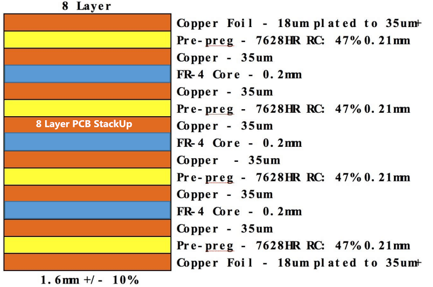
The fabrication process begins by cleaning the surface of the prototype boards. This step is necessary for the board to pass the solder mask application process. Next, we must clean the board to remove the ink epoxy and solder mask film covering the surface. This stage is critical as we expose the board to UV light, which penetrates through the photo film protecting the exposed copper. After this, the board goes into an oven to cure the solder mask.
Next, the design will move to a board layout. In schematics, each symbol has a corresponding pattern. Using the land pattern, the board layout is ready for fabrication. This step defines the board outline, positions components, and creates connections in copper.
After the design is complete, the PCB goes through a series of steps. First, it undergoes a resist-stripping process. This step is necessary for boards that have more than two layers. If the board is a simple two-layer design, it will skip this step.
The Gerber file is a universally accepted format for PCB prototyping. These Gerber files contain information that engineers send to PCB manufacturers. These files can have multiple layers, depending on the PCB stack-up, drill program, and pick-and-place layout. The Gerber files also contain fabrication drawings. A Gerber file is necessary for each copper circuit.
Bonding of PCB prototypes
A full-circuit board fabrication cycle is a multi-step process. The first step is to drill the PCB minimum hole size. This process can involve drilling more than 100 holes in one PCB. Then, we expose the circuit board to a chemical bath, which deposits copper traces over the entire panel and inside the hole. The next step is to prepare the panel for solder masking, which involves using epoxy solder mask ink and UV lighting.
A complete printed circuit board fabrication cycle is crucial in the development process. The PCBs are typically made up of various layers, depending on the product. They may contain as few as four layers or as many as eight. In addition, the thickness of the prototype PCB will vary from 0.4 millimeters to two millimeters. A full prototype PCB fabrication cycle will require a bill of materials (BOM) and a detailed list of components and raw materials.
Inspection of prototype PCBs
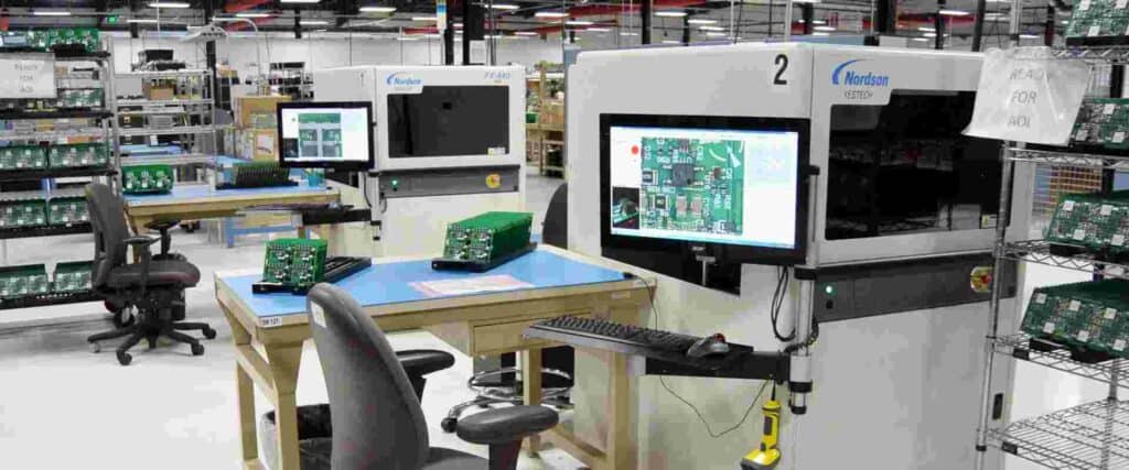
Visual inspection is a common testing method for circuit boards, but it can be inaccurate and time-consuming. Visual inspection requires a magnifying glass or microscope, and the operator’s visual assessment will determine whether the PCB needs correction operations. However, there are limitations to visual inspection, such as human subjectivity and difficulty in collecting data.
The second type of inspection is the Time-Domain Reflectometer (TDR). This test uses an electromagnetic wave to look for failures on a PCB’s surface. Again, it’s important to use qualified technicians for this test. As a result, you’ll be able to offer a better product to your end users. This will also improve your brand authority and bottom line.
Components of a PCB Prototyping PCB
Several variations of PCB prototype boards exist in the market today. However, the most common variation is the single-sided PCB that has copper tracks that connect various components on the top side of the board. These types of PCBs are also known as single layer Printed Circuit Boards. However, double-sided and multilayer printed circuit boards also exist. The type you utilize depends upon the mock-up you want to generate.
Prototype PCBs comprise multiple elements. These elements include silkscreen, solder mask, copper, and FR4.
FR4
FR is a denotation that means flame retardation. Typically, FR4 is an epoxy resin that bears glass reinforcement to boost the material’s durability. By utilizing this part, manufacturers can give Prototype PCBs sufficient rigidity.
Copper
During every PCB production process, technicians must apply a copper laminate onto the board. The copper laminate helps technicians develop the complex circuitries you see on PCBs.
To accomplish copper lamination, technicians must utilize adhesive and heat. After this processing phase, the copper laminate sticks onto the board, ready for the next step.
You should also note that the number of copper laminate plates you utilize is directly proportional to the number of layers the PCB will have. Therefore, this is a crucial component.
Solder Mask
A solder mask is another crucial component that you will find on a PCB prototype. Technicians utilize this component to efficiently insulate copper traces, shielding them from external damage. Solder masks also shield the PCB’s copper from touching exterior metals hence preventing short circuits. Moreover, this component prevents liquid solder jumpers.
Silkscreen
The silkscreen is the last layer that you will find on a PCB. Technicians utilize this layer to imprint invaluable information onto the board. This information might include the board’s identification number, the company’s logos, etc.
Most technicians imprint info on the silkscreen layer using white paint. However, this is not the standard color. Therefore, you can find PCBs that bear writing in varying colors.
Prototype Printed Circuit Boards Pricing and Shipping Process
Before you choose where to manufacture, it is essential to understand how to price and ship prototype PCBs. This is because the success of your product depends on the quality of its components from your PCB partner. You can also check out the quality of their services by reading customer reviews and feedback. In addition to knowing the price of the prototype PCBs, you should also know their shipping and customer support policies.
The PCBs’ value pricing will vary according to same-day delivery quality, size, complexity, and design. You should also consider the number of tests you need. Once you have determined the number of tests and editing you need, you can proceed to the final quote. This will address any problems that might have occurred during the production process. You must also remember that not all manufacturers are available for every project. Each project requires a specific type of manufacturer.
Things to Consider Before Hiring a PCB Prototype Service

The PCB prototyping process can be an affordable option and fast to test your products and get a working prototype before you commit to manufacturing the product. This is a good option for medical devices that require a high level of accuracy and reliability. Once you have a working prototype, you can test and change the design before manufacturing it. This will help you avoid a rude surprise during the manufacturing process.
A PCB prototyping process involves sending information about your project to a PCB prototype manufacturer. It is not necessary for every type of project, but it’s an excellent choice for testing new designs and performing quality checks. Listed below are some things to consider before hiring a PCB prototyping service.
