Water level indicators are useful tools in a variety of industries and applications, from monitoring water levels in tanks and reservoirs to ensuring proper drainage systems. One important aspect of designing a water level indicator is the printed circuit board (PCB). The PCB serves as the foundation for the electronic components that make up the water level indicator, allowing for accurate and reliable readings.
When designing a PCB for a water level indicator, there are several key factors to consider. These include the type of sensor being used, the desired accuracy of the readings, and the overall size and shape of the PCB. By carefully considering these factors and designing a PCB that meets the specific needs of the application, engineers can ensure that the water level indicator will function properly and provide accurate readings over time.
PCB Design
When designing a water level indicator, PCB design is an essential step. It helps in ensuring that the circuit is reliable and functions well. The following sub-sections discuss the two key aspects of PCB design: schematic design and PCB layout design.
Schematic Design
The schematic design is the first step in PCB design. It involves creating a circuit diagram that represents the components and connections in the circuit. The schematic design should be clear and easy to read. It should also include all the necessary components, such as resistors, capacitors, and transistors.
When designing the schematic, it is important to consider the power requirements, signal paths, and component placement. This ensures that the circuit functions as intended and is easy to troubleshoot if any issues arise.
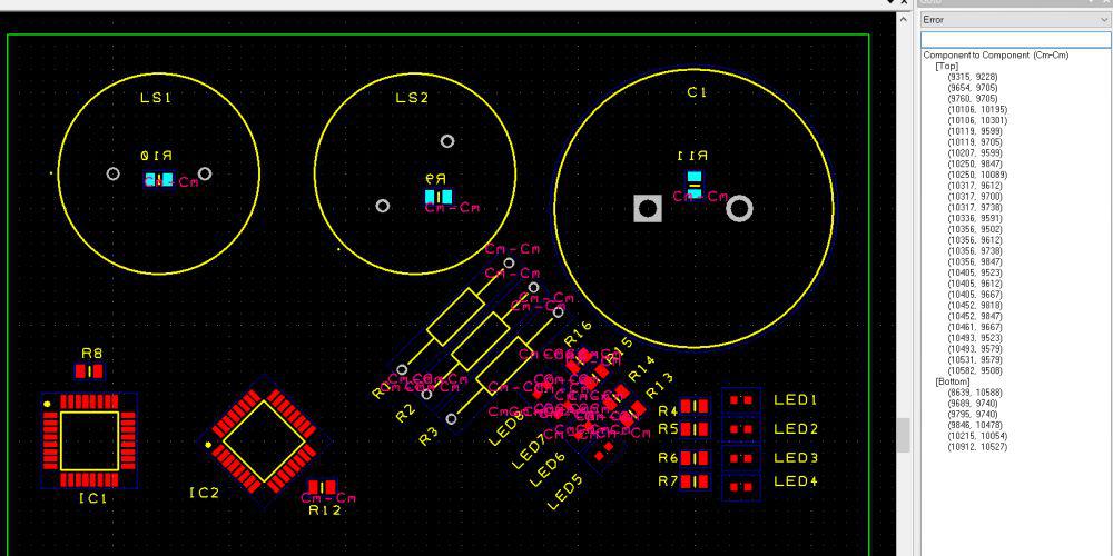
PCB Layout Design
The PCB layout design involves creating a physical representation of the circuit board. It involves placing the components on the board and routing the connections between them. The goal is to create a layout that is compact, efficient, and easy to manufacture.
When designing the PCB layout, it is important to consider the size of the board, the placement of the components, and the routing of the connections. It is also important to ensure that the board meets the required specifications, such as impedance and signal integrity.
To ensure that the PCB layout is accurate, it is recommended to use a PCB design software. These tools help in creating a precise layout and can detect any errors in the design.
In conclusion, PCB design is a critical step in designing a water level indicator. The schematic design and PCB layout design are two key aspects of the process. By following the best practices and using the right tools, it is possible to create a reliable and efficient circuit board.
Water Level Indicator

A water level indicator is an electronic device used to measure the level of water in a tank or reservoir. It is commonly used in households, industries, and agriculture to monitor water levels and prevent overflow or dry running of pumps. In this section, we will discuss the working principle and components used in a water level indicator based on PCB design.
Working Principle
The working principle of a water level indicator is based on the conductive properties of water. In this design, we use a set of probes made of conductive metal that are placed at different levels in the tank. When the water level rises and comes in contact with the probes, it completes the circuit and sends a signal to the indicator unit. The indicator unit then displays the water level on a digital or analog display.
Components Used
The following components are used in a water level indicator based on PCB design:
-
Microcontroller: A microcontroller is the brain of the system that controls the overall functioning of the device.
-
Probes: Probes are made of conductive metal and are placed at different levels in the tank to detect the water level.
-
Display: A display unit is used to display the water level in a digital or analog format.
-
Power Supply: A power supply unit is used to provide power to the system.
-
Resistors and Capacitors: Resistors and capacitors are used to regulate the current and voltage in the system.
-
Transistors: Transistors are used to amplify the signal and drive the display unit.
In conclusion, a water level indicator based on PCB design is a simple and effective way to monitor the water level in a tank or reservoir. By using conductive probes and a microcontroller, the device can accurately measure the water level and prevent overflow or dry running of pumps.
Testing and Troubleshooting
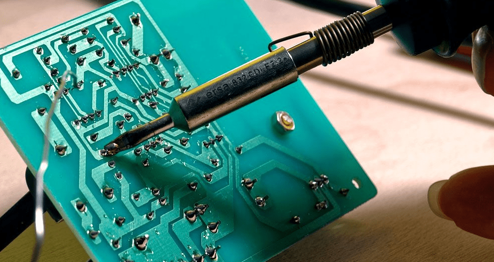
After completing the PCB design for the water level indicator, it is important to test and troubleshoot the circuit to ensure that it functions properly. Testing and troubleshooting can help to identify any errors in the design or assembly process.
First, check the power supply and make sure that the voltage and current ratings are within the specified range. Use a multimeter to measure the voltage at different points in the circuit to ensure that the power is flowing correctly.
Next, test the individual components to ensure that they are working correctly. Use a continuity tester to check the connections between the components and the PCB. If there are any faulty components, replace them and retest the circuit.
Once the individual components have been tested, test the entire circuit. Apply power to the circuit and observe the output on the water level indicator. Check that the LED lights up when the water level reaches the desired level and turns off when the water level drops below that level.
If the circuit is not working correctly, use a troubleshooting guide to identify the problem. Check for loose connections, broken components, and incorrect wiring. Use a schematic diagram to compare the actual circuit with the expected circuit.
In conclusion, testing and troubleshooting are important steps in the PCB design process. By testing the individual components and the entire circuit, you can identify any errors and ensure that the circuit functions correctly. If there are any issues, use a troubleshooting guide to identify and fix the problem.
Conclusion
In conclusion, designing a PCB for a water level indicator requires careful consideration of various factors, including the type of sensor used, the power source, and the microcontroller. It is important to choose the right components and ensure that they are properly placed on the board to avoid interference and improve the overall performance of the device.
Throughout the design process, it is essential to follow best practices and guidelines for PCB layout and routing to minimize noise and ensure signal integrity. This includes optimizing trace widths and lengths, using ground planes, and avoiding sharp corners and right angles.
In addition, it is important to test the PCB thoroughly before deployment to ensure that it is functioning as expected and to identify any potential issues or errors. This can be done through various testing methods, including continuity testing, power testing, and functional testing.
Overall, designing a PCB for a water level indicator requires a combination of technical knowledge, attention to detail, and careful planning. By following best practices and guidelines, designers can create a reliable and efficient device that meets the needs of their clients or users.
