Table of Contents
TogglePrinted Circuit Board (PCB) design and manufacturing is a crucial aspect of modern electronics. PCBs are used in a wide range of electronic devices, from smartphones and laptops to medical equipment and aerospace systems. PCBs provide a compact, reliable, and cost-effective means of connecting and powering electronic components.
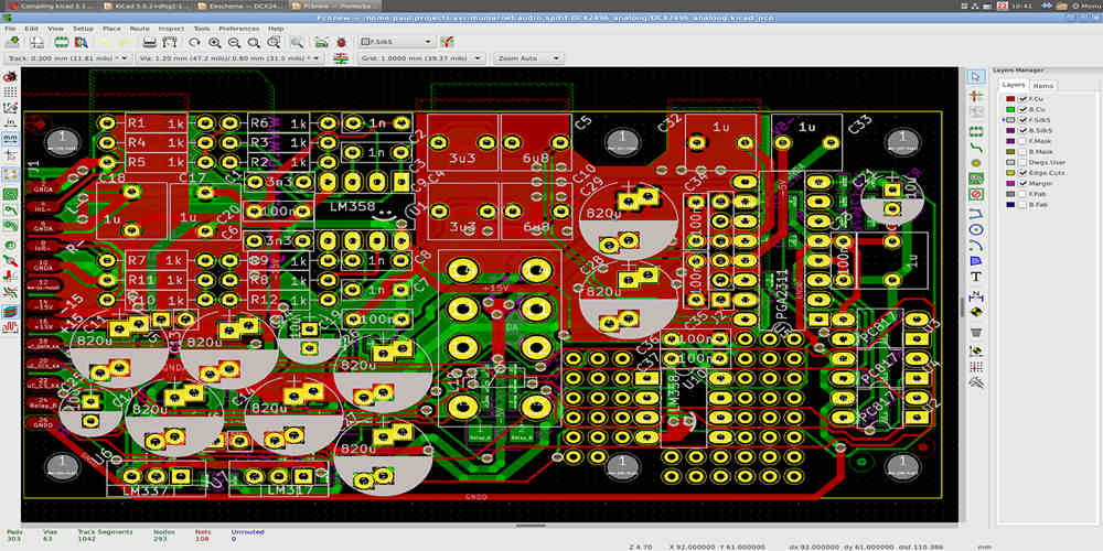
Designing a PCB involves creating a layout of the components and their connections on a board. This layout is then used to manufacture the PCB, which involves etching the connections onto a board and adding the components. PCB design and manufacturing require expertise in electronics, computer-aided design (CAD), and manufacturing processes.
PCB design and manufacturing have come a long way since their inception in the 1940s. Today, designers have access to advanced CAD tools, simulation software, and manufacturing techniques that enable them to create complex, high-performance PCBs. In this article, we will explore the basics of PCB design and manufacturing, including the key steps involved, the tools and software used, and the latest trends and innovations in the field.

PCB Design
When designing a printed circuit board (PCB), there are several important steps to follow to ensure a successful end product. These steps include schematic capture, PCB layout, and design for manufacturability.
Schematic Capture
Schematic capture is the first step in the PCB design process. It involves creating a visual representation of the circuit using a schematic editor. This step is crucial because it allows the designer to ensure that the circuit is functioning as intended before moving on to the PCB layout.
During schematic capture, it is important to ensure that the circuit is easy to read and understand. This can be achieved by using clear labeling, organizing components logically, and minimizing the number of cross-overs and intersections.
PCB Layout
After the schematic is created, the next step is to lay out the PCB. This involves placing components on the board and routing traces to connect them. During this step, it is important to consider factors such as signal integrity, power distribution, and thermal management.
To ensure a successful PCB layout, it is important to follow design rules and guidelines. These rules may include minimum trace widths, clearance between components, and placement of decoupling capacitors.
Design for Manufacturability
Design for manufacturability (DFM) is the process of designing a PCB with the goal of making it easy and cost-effective to manufacture. This involves considering factors such as panelization, assembly, and testing.
During the DFM process, it is important to work closely with the manufacturer to ensure that the design is optimized for their specific processes. This can help to reduce the risk of errors and delays during production.
In conclusion, designing a PCB involves several important steps, including schematic capture, PCB layout, and design for manufacturability. By following these steps and working closely with the manufacturer, designers can ensure a successful end product.
PCB Manufacturing

When it comes to PCB manufacturing, there are several key steps that are critical to ensuring a successful end product. Some of the most important steps include CAM, drilling and plating, solder mask and silkscreen, testing, and inspection.
CAM
The first step in PCB manufacturing is the creation of a computer-aided manufacturing (CAM) file. This file contains all the necessary information for the PCB manufacturer to create the board, including the layout, drill holes, and any special features such as cutouts or slots.
Drilling and Plating
Once the CAM file is complete, the manufacturer uses it to drill holes in the board and add copper plating to the surface. This plating is essential for creating the circuitry that will be used to connect the components on the board.
Solder Mask and Silkscreen
After the drilling and plating is complete, the board is coated with a solder mask to protect the copper traces from oxidation and to prevent solder from flowing where it shouldn’t. The board is also printed with a silkscreen layer, which adds text and graphics to the board to help identify components and connections.
Testing and Inspection
Once the board is complete, it undergoes a series of tests and inspections to ensure that it is functioning properly and meets all necessary specifications. This includes both visual inspections and electrical testing to ensure that all connections are sound and that the board meets all necessary tolerances.
Overall, PCB manufacturing is a complex process that requires careful attention to detail at every step. By following these key steps and using high-quality materials and equipment, manufacturers can create PCBs that meet the needs of their customers and provide reliable performance over the long term.

