PCB layout design for power supply circuits is a crucial aspect of electronic design. It involves the placement of components and routing of connections to ensure the power supply can deliver the required voltage and current to the load. A poorly designed layout can result in performance issues, noise, and even damage to the components.
The first step in designing a power supply circuit is to determine the requirements of the load. This includes the voltage and current needed, as well as any other specifications such as ripple and noise. Once the requirements are known, the designer can choose the appropriate components and begin the layout design. Factors such as component placement, trace width, and ground plane design must be considered to ensure proper functionality and reliability of the power supply circuit.
Power Supply Circuit Design
Overview
The power supply circuit is one of the most important components in any electronic system. It provides the necessary voltage and current to power the system’s components and ensure proper functioning. The design of a power supply circuit for a PCB requires careful consideration of various factors to ensure its reliability, efficiency, and safety.
Design Considerations
When designing a power supply circuit, several factors must be considered. The following are some of the most important considerations:
-
Voltage and current requirements: The power supply circuit must be designed to meet the voltage and current requirements of the system’s components.
-
Efficiency: The power supply circuit must be designed to minimize power loss and maximize efficiency.
-
Heat dissipation: The power supply circuit must be designed to dissipate heat efficiently to prevent overheating and damage to the system.
-
Safety: The power supply circuit must be designed to ensure safety and prevent electrical hazards.
Schematic Design
The schematic design is the first step in designing a power supply circuit for a PCB. The following are some of the key components that should be included in the schematic design:
-
Transformer: The transformer is used to step up or step down the voltage to the required level.
-
Rectifier: The rectifier is used to convert the AC voltage from the transformer to DC voltage.
-
Capacitor: The capacitor is used to smooth out the DC voltage and reduce ripple.
-
Regulator: The regulator is used to regulate the output voltage to the required level.
-
Protection circuitry: The protection circuitry is used to prevent overvoltage, overcurrent, and short circuits.
In conclusion, designing a power supply circuit for a PCB requires careful consideration of various factors, including voltage and current requirements, efficiency, heat dissipation, and safety. The schematic design is the first step in the process and should include key components such as the transformer, rectifier, capacitor, regulator, and protection circuitry.
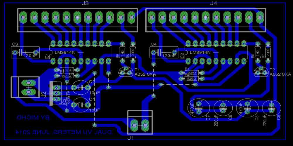
PCB Layout Design

When designing a power supply circuit, the PCB layout is crucial to ensuring that the circuit operates effectively and reliably. The following sub-sections outline some important considerations when designing the PCB layout for a power supply circuit.
Placement of Components
Proper placement of components is essential for good PCB layout design. Components should be arranged in a logical and organized manner to minimize the length of the traces and reduce the possibility of interference.
Routing Guidelines
Routing guidelines should be followed to ensure that the power supply circuit operates effectively and reliably. High current traces should be kept as short and wide as possible to reduce resistance and minimize voltage drops. Signal traces should be kept away from high current traces to avoid interference.
Ground Planes and Power Planes
Ground planes and power planes are important for power supply circuits. Ground planes help to reduce noise and provide a low impedance path for the return current. Power planes help to distribute power to the components more efficiently.
EMI/EMC Considerations
Electromagnetic interference (EMI) and electromagnetic compatibility (EMC) are important considerations when designing the PCB layout for a power supply circuit. EMI can cause interference with other circuits, while EMC ensures that the circuit operates effectively in its environment. Shielding, filtering, and grounding techniques can be used to minimize EMI and ensure EMC.
In summary, the PCB layout design is crucial to ensuring that a power supply circuit operates effectively and reliably. Proper placement of components, routing guidelines, ground planes and power planes, and EMI/EMC considerations are important factors to consider when designing the PCB layout for a power supply circuit.
Design Verification

Before moving on to the manufacturing process, it is important to verify the design of the power supply circuit. This ensures that the circuit will function as intended and avoids any potential issues or failures.
Design Rule Check
The first step in design verification is to perform a Design Rule Check (DRC). This involves checking the layout against a set of predefined rules and constraints, such as minimum trace width, spacing, and clearance. This ensures that the layout meets the requirements for the manufacturing process and avoids any potential issues or failures.
Signal Integrity Analysis
Signal Integrity (SI) analysis is another important step in design verification. This involves analyzing the behavior of signals in the circuit, such as voltage and current, to ensure that they are within acceptable limits. This helps to avoid any potential issues or failures, such as noise or distortion in the output.
Thermal Analysis
Thermal analysis is also a crucial step in design verification, especially for power supply circuits. This involves analyzing the temperature distribution in the circuit to ensure that it does not exceed the maximum operating temperature of the components. This helps to avoid any potential issues or failures, such as component damage or malfunction.
In conclusion, design verification is an essential step in the PCB layout design process for power supply circuits. Performing a Design Rule Check, Signal Integrity Analysis, and Thermal Analysis helps to ensure that the circuit will function as intended and avoids any potential issues or failures.
