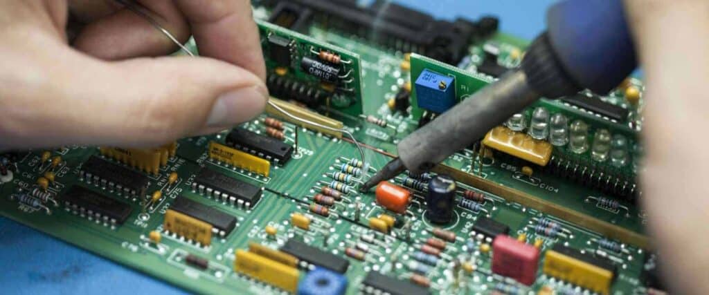
Printed Circuit Board (PCB) modeling is an essential aspect of the electronics industry. It involves designing and simulating the behavior of a PCB before it is manufactured. PCB modeling allows engineers to identify potential issues with the design, such as signal interference, power consumption, and thermal management, and address them before the board is produced. This process saves time and money while ensuring the final product performs as intended.
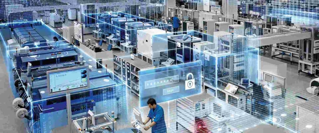
PCB modeling has become increasingly important as technology advances and circuitry becomes more complex. With the rise of Internet of Things (IoT) devices, 5G networks, and artificial intelligence (AI) applications, PCBs must meet higher performance standards than ever before. Modeling software enables engineers to accurately predict how a PCB will behave under various conditions, allowing them to optimize the design for maximum performance and efficiency.
In this article, we will explore the fundamentals of PCB modeling, including the different types of software available and the benefits of using modeling in the design process. We will also discuss common challenges and considerations when modeling a PCB and provide tips for successful modeling. Whether you are a seasoned engineer or new to the field, understanding the importance of PCB modeling can help you create better designs and improve your overall workflow.
Overview of PCB Modeling
What is PCB Modeling?
PCB modeling is the process of creating a three-dimensional model of a printed circuit board (PCB) using computer-aided design (CAD) software. The model includes the physical components, traces, vias, and other features of the PCB. PCB modeling is an important step in the design and manufacturing of PCBs, as it allows engineers to visualize and analyze the layout and functionality of the board before it is physically produced.
Why is PCB Modeling Important?
PCB modeling is important because it allows engineers to identify and correct design flaws before the board is manufactured. By creating a virtual model of the board, engineers can test the electrical performance, thermal properties, and mechanical stability of the design. This helps to reduce the risk of costly errors and ensures that the final product meets the required specifications.
Applications of PCB Modeling
PCB modeling is used in a wide range of applications, including:
- Designing and prototyping new PCBs
- Analyzing and optimizing the performance of existing PCBs
- Simulating the behavior of PCBs under different environmental conditions
- Identifying and resolving design issues before production
- Creating documentation and assembly instructions for PCBs
In addition to these applications, PCB modeling is also used in industries such as aerospace, automotive, and telecommunications, where the reliability and performance of PCBs are critical.
Overall, PCB modeling is an essential tool for PCB design and manufacturing, allowing engineers to create and test complex designs with greater accuracy and efficiency.
Types of PCB Modeling

Analytical Modeling
Analytical modeling is a type of PCB modeling that uses mathematical equations to predict the behavior of a PCB. This type of modeling is based on the assumption that the PCB is a simple structure that can be described by a set of governing equations. Analytical modeling is often used to predict the behavior of simple PCB structures, such as transmission lines and capacitors.
One advantage of analytical modeling is that it is relatively fast and inexpensive compared to other types of modeling. However, it is limited in its ability to accurately predict the behavior of complex PCB structures, such as multi-layer PCBs.
Numerical Modeling
Numerical modeling is a type of PCB modeling that uses computer simulations to predict the behavior of a PCB. This type of modeling is based on the finite element method (FEM) or finite difference method (FDM), which breaks the PCB down into small elements or cells that can be analyzed individually.
Numerical modeling is more accurate than analytical modeling and can be used to predict the behavior of complex PCB structures. However, it is more computationally intensive and time-consuming than analytical modeling.
Empirical Modeling
Empirical modeling is a type of PCB modeling that is based on experimental data. This type of modeling involves measuring the behavior of a PCB under different conditions and using the data to develop a model that can predict the behavior of the PCB under similar conditions.
Empirical modeling is useful when analytical or numerical modeling is not possible or when the accuracy of these models is uncertain. However, empirical modeling is limited by the availability and quality of experimental data.
In summary, there are three main types of PCB modeling: analytical modeling, numerical modeling, and empirical modeling. Each type of modeling has its advantages and limitations, and the choice of modeling method depends on the complexity of the PCB structure and the accuracy required for the analysis.
PCB Modeling Techniques
When it comes to modeling printed circuit boards (PCBs), there are several techniques available. Each technique has its own strengths and weaknesses. In this section, we will discuss some of the most commonly used PCB modeling techniques.
Finite Element Analysis (FEA)
Finite Element Analysis (FEA) is a widely used technique for modeling PCBs. It involves dividing the PCB into small elements and solving the equations for each element. This technique is useful for modeling complex geometries and materials. It is also useful for analyzing the effects of temperature and mechanical stress on the PCB.
Boundary Element Method (BEM)
Boundary Element Method (BEM) is another popular technique for modeling PCBs. It involves dividing the PCB into surfaces and solving the equations for each surface. This technique is useful for modeling electromagnetic fields and radiation. It is also useful for analyzing the effects of external electromagnetic fields on the PCB.
Transmission Line Matrix (TLM)
Transmission Line Matrix (TLM) is a technique for modeling PCBs that involves dividing the PCB into small cells and solving the equations for each cell. This technique is useful for modeling high-frequency circuits and transmission lines. It is also useful for analyzing the effects of noise and interference on the PCB.
Method of Moments (MoM)
Method of Moments (MoM) is a technique for modeling PCBs that involves dividing the PCB into small elements and solving the equations for each element. This technique is useful for modeling antennas and other radiating structures. It is also useful for analyzing the effects of external electromagnetic fields on the PCB.
In conclusion, there are several techniques available for modeling PCBs, each with its own strengths and weaknesses. The choice of technique depends on the specific requirements of the project.
Tools for PCB Modeling

When it comes to PCB modeling, there are a variety of tools available for both software and hardware. Here are some of the most commonly used tools for PCB modeling:
Software Tools for PCB Modeling
-
Altium Designer: This is a powerful software tool that is widely used by PCB designers. It offers a range of features, including schematic capture, PCB layout, and design rule checks. It also has a user-friendly interface that makes it easy to use.
-
Eagle PCB Design: This is another popular software tool for PCB modeling. It offers a range of features, including schematic capture, PCB layout, and design rule checks. It also has a large library of components that makes it easy to design PCBs.
-
KiCAD: This is a free, open-source software tool that is widely used by PCB designers. It offers a range of features, including schematic capture, PCB layout, and design rule checks. It also has a large library of components that makes it easy to design PCBs.
Hardware Tools for PCB Modeling
-
Oscilloscope: This is a hardware tool that is used to measure the voltage and current of a circuit. It is essential for PCB modeling because it allows designers to see how the circuit is behaving.
-
Logic Analyzer: This is another hardware tool that is used to measure the voltage and current of a circuit. It is particularly useful for debugging digital circuits.
-
Multimeter: This is a basic tool that is used to measure voltage, current, and resistance. It is essential for PCB modeling because it allows designers to test the various components of the circuit.
In conclusion, the tools for PCB modeling include both software and hardware tools. The software tools include Altium Designer, Eagle PCB Design, and KiCAD, while the hardware tools include oscilloscopes, logic analyzers, and multimeters. These tools are essential for PCB modeling and can help designers create high-quality PCB designs.
