PCB power supply layout is a critical aspect of electronic design that can significantly impact the performance and reliability of a circuit. The layout of the power supply components on a printed circuit board (PCB) can affect the noise, ripple, and stability of the power output, as well as the overall efficiency and durability of the system.
The proper placement and routing of power supply components such as capacitors, inductors, and voltage regulators can help to reduce noise and ripple, improve voltage regulation, and prevent thermal issues. Careful attention to the physical layout of the PCB can also help to minimize electromagnetic interference (EMI) and ensure proper grounding, which is essential for reliable operation. In addition, proper power supply layout can help to improve the overall performance and longevity of the circuit, while also reducing the risk of failure or damage.
PCB Power Supply Layout Basics
When designing a printed circuit board (PCB) power supply, there are several important factors to consider. Proper power supply layout is essential for ensuring reliable and efficient operation of electronic devices. Here are some basic guidelines to follow when designing a PCB power supply layout:
Component Placement
The placement of components on a PCB can have a significant impact on the performance of the power supply. It is important to place components in a way that minimizes noise and interference. Here are some tips for component placement:
- Place the power supply components as close to the power input as possible.
- Keep high-current components, such as inductors and capacitors, away from sensitive components, such as op-amps and ADCs.
- Use ground planes and keep sensitive components away from noisy areas of the board.
Trace Routing
The routing of traces on a PCB is another important consideration when designing a power supply layout. Here are some tips for trace routing:
- Use wide traces for high-current paths.
- Keep traces as short and direct as possible.
- Avoid sharp corners and right angles, as they can cause impedance and noise issues.
- Use a ground plane to reduce noise and improve signal integrity.
Decoupling Capacitors
Decoupling capacitors are used to filter out noise and provide stable power to sensitive components. Here are some tips for decoupling capacitor placement:
- Place decoupling capacitors as close to the power pins of sensitive components as possible.
- Use multiple capacitors of different values to cover a wide range of frequencies.
- Use low-ESR (Equivalent Series Resistance) capacitors for high-frequency noise filtering.
By following these basic guidelines, you can design a reliable and efficient PCB power supply layout.
Grounding and Decoupling
Grounding and decoupling are two critical aspects of PCB power supply layout. Proper grounding ensures that all components on the board are at the same potential, while decoupling capacitors help to filter out any noise that may be present on the power supply lines.
Grounding
When designing the grounding scheme for a PCB, it is important to consider the location of the power supply and the ground plane. It is best to keep the power supply and ground plane as close together as possible to minimize the inductance between them. This can be achieved by placing the power supply and ground plane on adjacent layers of the PCB.
In addition, it is important to ensure that all components on the board are properly grounded. This can be achieved by connecting each component’s ground pin to the ground plane using short traces. It is also important to minimize the loop area of the ground connections to further reduce any potential noise.
Decoupling
Decoupling capacitors are used to filter out any noise that may be present on the power supply lines. These capacitors should be placed as close as possible to the power supply pins of each component. The value of the decoupling capacitor should be chosen based on the frequency of the noise that needs to be filtered out.
It is also important to use multiple decoupling capacitors of different values to filter out noise at different frequencies. For example, a 0.1uF capacitor can be used to filter out high-frequency noise, while a 10uF capacitor can be used to filter out low-frequency noise.
In conclusion, proper grounding and decoupling are critical aspects of PCB power supply layout. By following these guidelines, you can minimize noise and ensure that your power supply is stable and reliable.
Component Placement

The placement of components on a PCB is crucial for the performance and reliability of the power supply. Proper component placement can minimize noise, reduce electromagnetic interference (EMI), and improve thermal management.
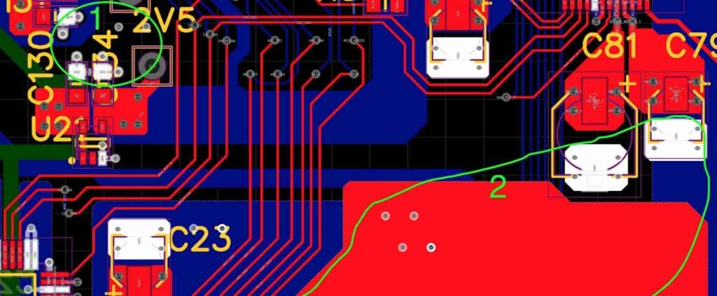
One of the most important considerations for component placement is the distance between high-current components. Components that draw high currents, such as inductors and capacitors, should be placed as close to each other as possible to minimize the loop area and reduce the parasitic inductance and resistance. This can improve the efficiency and stability of the power supply.
Another important consideration is the placement of the input and output capacitors. Input capacitors should be placed as close as possible to the input terminals to filter out high-frequency noise and prevent voltage spikes. Output capacitors should be placed as close as possible to the load to provide stable voltage regulation and reduce the output ripple.
In addition, the placement of the power switch and the diode can also affect the performance of the power supply. The power switch should be placed close to the input capacitors to minimize the loop area and reduce the switching losses. The diode should be placed close to the output capacitors to minimize the voltage drop and reduce the reverse recovery time.
Overall, proper component placement is essential for the performance and reliability of the power supply. By considering the distance between high-current components, the placement of input and output capacitors, and the placement of the power switch and diode, designers can optimize the layout of the power supply and improve its efficiency, stability, and EMI performance.
Traces and Copper Pour
One of the most important aspects of PCB power supply layout is the design of the traces and copper pour. These elements play a critical role in ensuring that the power supply functions properly and efficiently.
Traces
Traces are the conductive paths that connect the various components in the power supply. When designing traces, it is important to consider the current carrying capacity of the trace, the voltage drop across the trace, and the impedance of the trace.
To ensure that the traces can handle the current, it is important to use a trace width calculator to determine the appropriate width for the trace. This will prevent the trace from overheating and potentially causing damage to the power supply.
Copper Pour
Copper pour is a technique used to create a large, low-impedance ground plane that can improve the performance of the power supply. By creating a copper pour around the power supply components, it is possible to reduce the loop area and minimize the effects of electromagnetic interference.
When creating a copper pour, it is important to ensure that the pour is connected to ground and that it does not interfere with the traces or other components on the board. It is also important to consider the size of the pour and the distance between the pour and other components.
Overall, the design of the traces and copper pour is critical to the performance of the power supply. By carefully considering the current carrying capacity, voltage drop, impedance, and other factors, it is possible to create a power supply that is efficient, reliable, and effective.
Thermal Considerations
When designing a PCB power supply layout, thermal considerations are crucial to ensure the reliability and longevity of the system. Excessive heat can cause components to fail prematurely and reduce the overall efficiency of the power supply. Here are some factors to consider when addressing thermal issues in your layout:
Component Placement
The placement of components can have a significant impact on the thermal performance of the power supply. Components that generate more heat, such as voltage regulators and power transistors, should be placed in areas with good airflow and heat dissipation. Placing components too close together can also lead to thermal issues, so it’s important to space them out appropriately.
Heat Sinks
Heat sinks are a common solution for dissipating heat from power components. They work by increasing the surface area available for heat transfer, allowing the heat to be dissipated more efficiently. When selecting a heat sink, it’s important to consider the power dissipation requirements of the component and choose a heat sink that can handle the necessary thermal load.
Thermal Pads
Thermal pads are another useful tool for managing heat in a power supply layout. They are placed between the component and the PCB to improve heat transfer and reduce the thermal resistance between the two surfaces. When using thermal pads, it’s important to ensure that they are the correct size and thickness for the component being used.
Trace Width and Copper Pour
The width of traces and the use of copper pours can also impact the thermal performance of a power supply layout. Wider traces and larger copper pours can help dissipate heat more effectively, reducing the temperature of the components. However, it’s important to balance this with other design considerations, such as board size and cost.
In conclusion, thermal considerations are an important aspect of PCB power supply layout design. By carefully considering component placement, heat sinks, thermal pads, trace width, and copper pours, designers can create a system that is reliable, efficient, and long-lasting.
EMI and EMC Considerations
When designing a power supply layout, it is important to consider electromagnetic interference (EMI) and electromagnetic compatibility (EMC). EMI refers to the unwanted electromagnetic radiation emitted by electronic devices, while EMC refers to the ability of a device to operate without interfering with other devices.
To reduce EMI, it is important to minimize the loop area of the power supply circuit. This can be achieved by keeping the input and output traces as short as possible and avoiding large loops. Additionally, it is recommended to use a ground plane and to place the power supply components close to each other.
To ensure EMC compliance, it is important to use components that meet the necessary standards. This includes using components that have been tested for emissions and immunity, and ensuring that the power supply layout meets the necessary clearance and creepage requirements.
Another important consideration is the use of shielding. Shielding can help to reduce EMI by blocking electromagnetic radiation. This can be achieved by using a metal enclosure or by adding shielding to the PCB layout.
In summary, when designing a power supply layout, it is important to consider EMI and EMC. This can be achieved by minimizing the loop area, using components that meet the necessary standards, and using shielding if necessary.
High Voltage Considerations
When designing a PCB power supply layout, it’s important to consider high voltage considerations. High voltage can pose a risk of electrical shock to users, and can also damage components if not properly handled.
To ensure safety and proper functionality, consider the following high voltage considerations:
-
Isolation: High voltage components should be isolated from low voltage components to prevent electrical shock and damage. This can be achieved through physical separation or the use of isolation barriers.
-
Clearances: High voltage components should have adequate clearance from other components and conductive surfaces to prevent arcing and electrical discharge. The required clearance will depend on the voltage level and environmental conditions.
-
Creepage: Creepage is the distance between two conductive surfaces along the surface of a PCB. High voltage components should have sufficient creepage distance to prevent arcing and electrical discharge.
-
Trace width: High voltage traces should be wider than low voltage traces to prevent voltage drop and overheating. The required trace width will depend on the current level and environmental conditions.
-
Grounding: Proper grounding is essential for high voltage circuits to prevent electrical shock and ensure proper functionality. Grounding should be done in accordance with industry standards and best practices.
By considering these high voltage considerations, you can design a safe and reliable PCB power supply layout.
