A fascinating and quickly expanding area of the PCB manufacturing industry is radio frequency printed circuit boards (RF PCBs). An RF circuit board is any high-frequency printed circuit board that operates at a frequency of 100 MHz or higher, according to the industry that produces printed circuit boards (PCBs).
Anything with a radio frequency that is higher than 2 GHz is considered to be a microwave PCB. The radio frequency at which they function is the key distinction between RF circuit boards and Microwave PCBs. RF boards operating at a frequency greater than 2GHz are categorized as microwave PCBs.
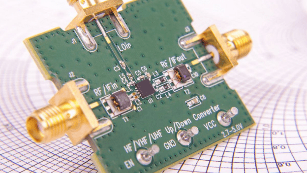
Any application that calls for receiving and transmitting radio signals uses RF boards and microwave PCBs for communication signals. Radar stations and cell phones are two examples of common applications.
In particular, RF transmissions are susceptible to noise. Thus, the possibility of signal ripple or reflection is common. The need to adjust the impedance value along each of the circuit’s traces makes impedance a particularly important factor in this class of circuits.
Additionally, it’s important to limit the power losses brought on by signal reflections by designing appropriate paths for return current, which, as frequency rises, prefers to take the routes with the lowest inductance.
Crosstalk, which is the energy transfer between adjacent traces brought on by inductive or capacitive couplings, becomes more important as the performance and density of the components rise.
RF PCB design requires taking into account material properties like the dissipation factor and dielectric constant. When compared to materials designed for high frequencies, FR-4 has a larger dissipation factor, resulting in significant insertion losses that rise with frequency.
Additionally, as the frequency rises, the FR-4’s dielectric constant might rise by up to 10%, causing impedance fluctuations throughout the PCB traces.
Best Practices for RF PCB Design
Material Selection
Although materials like FR-4, which are frequently used in PCB fabrication, are very affordable, they are not the best option for high-frequency RF applications due to the non-uniformity of the dielectric constant and a lower tangent angle.
Specific materials are used for RF PCB design. materials include ceramic, PTFE, hydrocarbons, and several kinds of glass fiber. The PFE and PTFE materials, which are members of the fluoropolymer family, enhance the base material’s chemical resistance and possess anti-adhesion, smoothness, and exceptional heat resistance qualities.
Even at temperatures of 200 °C, they are resistant. The ideal option is PTFE with fiberglass if money is not an issue and quality is more essential than cost.
The ceramic-coated PTFE is used because it is cheaper and requires a simplified production method. Although Rogers materials are more expensive, they allow for power losses to be reduced by about 50%, ensuring great performance even over 20GHz and a low dielectric constant value that is stable and reproducible as the frequency changes.
The most common methodology is to use various materials that fulfill the requirements for electrical performance, thermal properties, and cost because RF PCBs are often multi-layered.
For instance, the exterior layers can be made from high Rogers laminates, whereas the inside layers can be made of less expensive epoxy glass laminates.
Transmission Lines
RF transmission lines for RF PCBs must have their impedance value rigorously managed to prevent power losses and guarantee signal integrity. The characteristic impedance in microstrip transmission lines is determined by the trace width, layer thickness, and type of dielectric.
Strip lines are used on the inner layers, and microstrips are used on the outer layers. In contrast, coplanar waveguides offer the highest level of isolation, particularly when it comes to RF signals that cross very close traces.
Understanding the importance of the knowledge of the precise value of the dielectric constant of each layer, one of the many tools readily available online may be used to compute the characteristic impedance and, in turn, the width of the trace.
Impedance and Inductance
One strategy that is typically applied by designers is to set a benchmark impedance value, usually 50 ohms, and then only RF components that have this particular impedance are selected.
Given that it is prominently used, this value makes impedance matching easier, enabling each PCB trace to be given the proper width. However, inductance should be maintained as low as possible because this can significantly affect the RF PCB design.
All of that is accomplished by equipping each RF component with a suitable ground connection via multiple through holes and ground planes that are sizable and gap-free. High-frequency elements and traces need to be placed close to ground planes.
Routing
The first rule relates to the curvature and angles of a trace. It is ideal to generate an arc with a curvature radius that is more than 3 times the trace width when an RF transmission line needs to change direction due to routing necessities.
This makes it so that the characteristic impedance is guaranteed to remain unchanged throughout the curvilinear segment. If this isn’t realizable while keeping in mind that right angles must be replaced by two 45° degrees, draw a suitable angle.
It is recommended to install at least two through holes for each crossing of a transmission line when it must cross through two or more layers to reduce the consequent discrepancy in inductance.
When utilizing a via pair with the maximal diameter value compatible with the trace width for the holes, the inductance variation can be lowered by 50 percent. When crossed by sensitive signals, it is very important to have the traces linking the RF components as short as possible, properly spaced away, and oriented orthogonally on the next layers.
The four-layer multilayer construct is the best option for the stackup. Although more expensive than a double-layer approach, the outcomes are far superior and are simple to duplicate. High frequencies cannot tolerate the discontinuities of the ground planes; therefore, continuous ground planes must be introduced beneath the RF signal traces.
Insulation
It’s crucial to pay attention to prevent bad couplings between the signals. The RF transmission lines shouldn’t run parallel for extended periods and should be kept as far from other traces as feasibly as can be. In reality, as the distance between them decreases and the distance traveled in the parallel direction rises, the coupling between parallel microstrips tends to grow.
Similarly to this, traces carrying high-power signals must also be segregated from other circuit components. Using the grounded coplanar waveguides, one can achieve an outstanding insulation value.
To prevent coupling problems, traces carrying high-speed signals ought to be routed on a distinct layer from RF signals. By incorporating sufficient decoupling/bypass capacitors, the power supply lines should also be routed on designated layers.

Ground Planes
Instead of the usual method of inserting continuous ground planes side by side each other which contain transmission line parts, together with the rf components, rf traces can have via holes added to them. Via holes also help to prevent coupling between rf lines and other signals in the circuit board.
Bypass Capacitor
It is best to position bypass capacitors close to the power pins. In the center of the star, a decoupling capacitor with a higher capacity is positioned, and nearby each branch, other capacitors with a smaller capacity. This is especially helpful for components that have several pins arranged in a star pattern.
Given that this negates the decoupling action, special consideration must be given to the capacitor’s self-resonance frequency (SRF) value.
Components Ground Planes
For the majority of integrated circuits, the layer right beneath the component must have a continuous ground plane. This plane’s job is to direct the CC and RF signal return currents in the direction of the designated ground plane.
The ground paddle’s secondary job is to dissipate extra heat, so it needs to have the proper via holes. To increase dissipation, these vias should be through holes so they can cross multiple PCB layers.
How to manage the power in RF PCBs
A device requires more power to communicate the greater the amount of data required. Radio waves are constantly communicating with one another. This is accomplished through a device known as an RF Module, which is created by RF PCBs and receives radio signals between two or more devices.
The rf PCB design needs to control electricity. Avoid assembling the boards’ electrical parts in close proximity, even though it would be simpler.
Dealing with Loss Tangents in RF PCBs
High frequencies create extra heat during operation, which needs to be taken into consideration. A loss tangent is the term for this event. It describes a part of a multilayer board that becomes dense as a result of extra heat.
Monitoring the circuit’s amplitude is a simple way to fix this. When amplitude levels fall, more heat is produced.
