The latest generation of rigid-flex PCBs has a variety of applications. In addition to GPS equipment, they are essential in cell phones, computers, and tablets. They are also essential in medical devices such as X-rays, MRI systems, and heart monitors. Other uses for rigid-flex PCBs include temperature sensors and control tower instrumentation.
The advantages of rigid-flex PCB construction include improved mechanical bend reliability. In particular, odd-layer-count constructions can minimize the flex area’s thickness and improve mechanical bend reliability. This approach also minimizes the cost of a PCB by maximizing its flexibility. Besides providing better mechanical bend reliability, rigid-flex PCBs also improve the reliability of electronic systems.
When it comes to rigid-flex PCBs, Altium offers two different modes. Its standard rigid-flex mode supports simple rigid-flex designs, while the Advanced Rigid-Flex mode, also known as “rigid-flex 2.0,” allows you to define overlapping stretches and flex regions. In addition, this new mode also supports custom splits and bookbinder-type structures.
The Future of Flexible Circuits
Soon, we will see a wide range of electronic devices with flexible circuits. For example, some foldable smartphones may have more durable displays thanks to flexible circuits. In addition, OLEDs, or organic light-emitting polymers, will be more helpful in televisions. The flexibility of OLEDs means they can be much thinner than LCDs. In addition, developing these flexible electronics could help make them easier to manufacture and reduce their overall cost.
Researchers are working to reduce their costs as these new circuits become more popular. While some rigid circuits are unsuitable for mass production, we can print others on various materials. However, it is necessary to remember that lithography techniques are not as effective on flexible substrates. Therefore, researchers are looking for environmentally friendly methods to manufacture these new circuits. The future of flexible circuits lies in the future.
Using flexible circuits in these applications opens up new opportunities for manufacturing. For example, automakers can improve production time by incorporating more compact electronic components and sensors. In addition, flexible circuits allow factories to use cheaper substrates, such as plastic film. This makes them less bulky, which is essential for industrial applications. These advances also provide new capabilities to industrial equipment. The future of flexible circuits is bright, and they are here to stay.
Rigid-Flex PCB Constructions
One type of rigid-flex PCB construction is the odd-layer construction, commonly used for designs requiring two-sided shielding. Most designs are driven by stripline impedance control, though EMI or RF considerations can also be important. This construction is often advantageous because it allows for high-density interconnects between rigid sections. Here are some characteristics of this type of construction.
An odd-layer construction has many layers on one side, while an even-layer construction has fewer layers on the other. An odd-layer construction gives the rigid area better flexibility while minimizing the thickness. In addition to the increased flexibility, the constructions are more reliable for mechanical bending. However, there are some advantages and disadvantages to both types of construction.
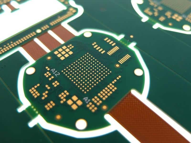
As the name implies, rigid-flex PCBs are PCBs with flexible sections connected to rigid sections. The flexible parts consist of different materials than the rigid ones. The rigid parts are conductive and non-conductive, but they must bond to the flexible sections with an adhesive. Moreover, the adhesive can be vulnerable to adhesive stresses and may cause damage to vias. If this happens, the flex sections may not function as intended.
Rigid-Flex PCB Constructions With Odd Layer Counts
Rigid-Flex PCB constructions with odd layer counts have several advantages over conventional designs. First, they provide improved mechanical bend reliability by minimizing the thickness of the flex area. As a result, they are often ideal for high-performance PCBs. But some caveats should be kept in mind. Rigid-Flex PCB constructions with odd layer counts may not be the most suitable for every project.
One of the main advantages of using rigid-flex circuits is that they can support buried vias and blind vias that connect the inner layers without passing through the outer layer. This means rigid-flex PCB constructions with odd layer counts can achieve higher packaging density. As a result, these boards can fit in narrower enclosures and are easier to manufacture. And despite these advantages, Rigid-Flex PCB constructions with odd layer counts must adhere to strict quality standards such as IPC 2223C.
In addition to the above advantages, Rigid-Flex PCB constructions with odd layer counts are easier to manufacture but require a higher cost. Moreover, rigid-flex PCB constructions with odd layer counts require careful engineering, especially in the areas of routing and bending. The advantages of this construction type include high reliability in extreme conditions, varying flex layer counts, and improved bend capabilities.
Asymmetrical Rigid-FleX PCB Constructions
Asymmetrical Rigid-FleX PCB constructions can meet a variety of design goals. These constructions are unique in their flexibility and rigidity. In addition to the above benefits, these constructions are less expensive than symmetrical PCBs. In addition, they can improve performance.
When designing rigid-flex PCBs, designers must pay particular attention to the bend area. For example, traces should be routed perpendicular to the bend line, and you should add dummy traces to strengthen the bend area.
Asymmetrical Rigid-FleX PCB constructions combine rigid and flexible layers. The flex area is thicker than the rigid ones, so it is essential to consider the layer count when designing your PCB. Rigid-Flex PCBs may require rigid layers in some areas. This construction type can help improve flexibility by minimizing the thickness of the flex area.
Asymmetrical Rigid-FleX PCB constructions can be manufactured with an odd layer count and offer many advantages. For example, an asymmetrical design requires fewer flex layers, reducing the design’s cost and complexity. It can also reduce the aspect ratio of blind vias. And it is easier to manufacture in an asymmetrical layout. And it doesn’t compromise reliability.
Variable Flex Layer Count

The term “variable flex layer count” refers to the number of layers in a flexible circuit. This type of circuit requires extra attention and consideration. The number and type of layers vary between manufacturers. For example, a two-layer FPC has a dozen different callouts for one zone. However, the two-number callouts for the adhesive and other material are not ranges but rather the thickness of the flexes before and after curing.
Variable Flex Layer Count construction is also known as asymmetrical or odd-number construction. This construction technique applies to both the rigid and flex parts of the PCB. It has the advantage of providing increased flexibility and mechanical bending reliability with minimum thickness. For example, asymmetrical designs reduce the aspect ratio of blind vias. However, this construction method may not suit your specific design needs.
With the latest innovations in flex circuit technology, you can now build a circuit with an unmatched range of flex layer counts. The wide range of flex layer counts is possible thanks to the use of a variety of construction methods. Blind, buried, and via in-pad technologies can all help vary flex layer count. Aside from increasing flexibility and mechanical bending properties, they also improve reliability. The flexibility and reliability of flex construction are crucial to a wide variety of electronic and wireless applications.
To achieve the highest flexibility, a varying Flex Layer Count is important. One of the advantages of this design technique is that the copper used in the PCB is distributed evenly throughout the layers. Therefore, by varying Flex Layer Count, you can maximize the number of flex layers while minimizing copper. An excellent way to mimic this approach is to use a loose leaf approach.
Integrated ZIF Tail Constructions
Integrated ZIF tail constructions are an excellent option for electrical cables that use pin connections. This configuration gives manufacturers a higher degree of flexibility when designing their products. They also save space in a confined space by eliminating the need for pin connections. Here’s what you need to know about this construction style.
Integrated ZIF tail constructions are an excellent choice for high-density applications. They reduce real estate by eliminating a separate rigid section for the ZIF connector. Moreover, they allow designers to reduce the thickness of the board while still achieving a high-density design. By eliminating the extra rigidity, these boards save space and money. Also, they are more reliable than other types of connectors.
Rigid-Flex Circuits With Blind Vias and Buried Vias
Blind vias and buried vias are common design elements in rigid-flex circuits. This type of circuit encapsulates the circuitry within a layered construction. Due to the limited flow characteristics of these circuits, a thicker No-Flow pre-preg is necessary for these designs. The increased pre-preg thickness has some implications for design, such as an increase in the aspect ratio of the blind vias.
The construction of these multilayer boards is similar to that of a traditional double-sided board. First, the layers are laminate with an outer layer and blind or buried vias drilled from layers two to seven. Then, the layers are stacked and pressed together. Depending on the type of multilayer circuit design, blind or buried vias are drilled from layers two to seven and from layers one to eight.
The use of blind or buried vias has numerous advantages for electronic devices. Among them are space savings, increased performance, and reduced size. Both types of vias are useful in electronic circuits, but the former is more expensive than the latter. While blind vias require multiple manufacturing steps and precision checks, buried vias are better for low-cost boards.
Flexible and rigid-flex PCBs are ideal for medical, military, and aerospace applications. These circuits enable designers to design circuitry that fits the device without adding bulk. Furthermore, rigid-flex PCBs are ideal for ultra-thin packaging and fine line technology. These boards can accommodate high-performance components. This is because they have low-loss properties.
Flexible Circuit With Air Gap Constructions
Air Gap Construction is an effective way of constructing a flexible circuit. Its natural radius is not restricted. This allows the flex pair to bend to their natural length without overlapping. However, when the air gap spacing is too small, the flex pairs may contact each other. This can cause the circuit to crack or fail.
Flex layers help create the circuit. In air gap constructions, the air gap separates the flex layers. This provides increased flexibility and reliability to the entire structure. It also reduces the thickness of the flex, preventing the “I-Beam” effect. In addition, each flex pair can bend on its thickness, unlike a traditional via. Thus, the Air Gap Constructions offer superior bending capabilities.
A multilayer flex circuit consists of three or more layers of conductors. They are interconnected through plated holes and may have openings to access lower circuit features. Depending on the desired flexibility, the layers are either laminated throughout the construction or are discontinuously laminated.
Multiple Rigid Area Thickness Construction
Parts with multiple rigid area thicknesses are a more complex form of construction. They can be manufactured in various ways but are typically limited to two or three rigid area thicknesses due to the required materials. In the most straightforward version, this is equivalent to manufacturing two boards. However, the number of layers required for multiple rigid area thicknesses may be more than one-half the thickness of each layer.
Each rigid area comprises three or more layers in multiple rigid area thickness constructions. These layers are generally evenly spaced between one another. This method has even layer counts so that vias do not go through the coverlay. The number of layers varies, ranging from four to sixteen. When using multiple flex layers, a single layer between two rigid sections is the air-gap layer.
Shielded Flex Layers Construction
One way to achieve shielding in flexible circuits is with copper shielding. While this shielding technique increases the thickness of the flex circuit, it also limits its bendability and raises the cost of the part. Unlike silver ink, this technique does not require additional layers of material. However, this construction method is less than ideal for circuits requiring controlled impedance.
Copper shielding is the most common type of shielding. Copper shield layers are copper etched to create a solid plane. Cross-hatched copper shields reduce flexibility by reducing shielding effectiveness. Copper shields are best for high-speed applications because they enable a controlled impedance signal. In addition, copper shields are often essential for multiple solutions. Copper shields are also a viable option if flexibility is a top priority.
The number of flex layers used in this construction varies depending on the size of the flexed section. For example, three or four flex layers sometimes join the first and second rigid sections. In other cases, there are two or three flex layers between the second and third rigid sections. This design is ideal for designs requiring two-sided shielding, stripline impedance control, and EMI and RF considerations.
