KiCad is a popular open-source software suite for electronic design automation (EDA). It provides a complete set of tools for designing printed circuit boards (PCBs) from schematics to layouts. With KiCad, designers can create professional-grade PCBs that are both functional and aesthetically pleasing.
One of the most important steps in designing a PCB is converting the schematic to a layout. KiCad offers a seamless workflow for this process, allowing designers to easily convert their schematics into PCB layouts. The software also provides a range of tools for optimizing the layout, including automatic routing, design rule checks, and 3D visualization. With KiCad, designers can ensure that their PCBs are both functional and optimized for manufacturing.
Overall, KiCad is a powerful and user-friendly tool for designing PCBs. Its seamless workflow, powerful tools, and open-source nature make it an ideal choice for both hobbyists and professionals alike. By using KiCad, designers can create high-quality PCBs that meet their specific needs and requirements.
Schematic Capture in KiCad
KiCad is a popular open-source software suite for electronic design automation (EDA) that allows users to create schematics, printed circuit board (PCB) layouts, and 3D models. The software provides a user-friendly interface for designing schematics and PCBs, allowing users to create complex designs with ease.
To start creating a schematic in KiCad, users can open the Eeschema application which is part of the KiCad suite. The application offers a wide range of tools and features that allow users to create and edit schematics quickly and efficiently.
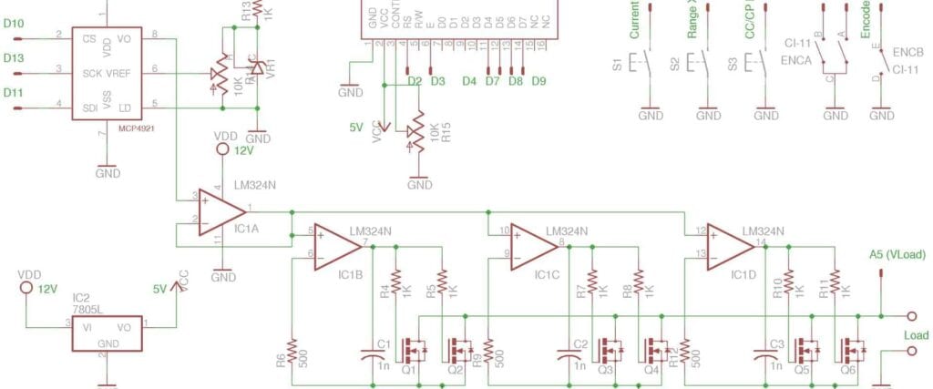
One of the most useful features of Eeschema is its hierarchical design capabilities. This allows users to create complex designs by breaking them down into smaller, more manageable sections. Users can create sub-sheets within a schematic, which can be interconnected to form a complete circuit.
Eeschema also offers a wide range of libraries containing pre-built symbols, footprints, and models for commonly used components. This makes it easy for users to add components to their schematics without having to create them from scratch.
Another useful feature of Eeschema is its ability to generate a netlist, which is a list of all the connections in a schematic. This netlist can be used to create a PCB layout in KiCad’s PCBnew application.
Overall, KiCad’s schematic capture capabilities are powerful and easy to use. With its hierarchical design capabilities, extensive library of pre-built components, and netlist generation, KiCad is an excellent choice for anyone looking to create complex schematics for their electronic designs.
Creating a New Project
Starting a New Project
To start a new project in KiCad, open the KiCad application and select “New Project” from the welcome screen. This will bring up a dialog box where you can specify the name and location of your new project. Once you have entered this information, click “OK” to create the new project.
Setting Up the Schematic
After creating a new project, the next step is to set up the schematic. To do this, first select “Schematic” from the project manager window. This will open a blank schematic sheet.
Before you begin designing your schematic, it’s important to set up the schematic preferences. To do this, go to “Preferences” > “Schematic Editor” and select the appropriate settings for your project. Some of the settings you may want to adjust include the grid size, the default font size, and the default line width.
Once you have set up your schematic preferences, you can begin designing your schematic. To add components to the schematic, select the appropriate component from the component library and place it on the schematic sheet. You can then connect the components using wires or buses.
Overall, setting up a new project in KiCad is a straightforward process. By following these steps, you can quickly create a new project and begin designing your schematic.
Creating the Schematic

Adding Components
To create a schematic in KiCad, the first step is to add components to the schematic editor. This can be done by selecting the component library from the left-hand side of the screen and then dragging and dropping the desired component onto the schematic editor. Alternatively, components can be added by using the “Place Component” option from the toolbar.
Connecting Components
Once the components have been added to the schematic editor, the next step is to connect them together. This can be done by using the “Place Wire” option from the toolbar. Simply click on the pin of one component and then click on the pin of another component to create a connection between them.
Adding Power and Ground Symbols
In addition to adding components and connecting them together, it is also important to add power and ground symbols to the schematic. This can be done by selecting the “Power” library from the left-hand side of the screen and then dragging and dropping the desired power symbol onto the schematic editor. The ground symbol can be added in the same way.
It is important to note that power symbols and ground symbols are not the same as regular components. They do not have pins that need to be connected to other components. Instead, they are used to indicate the presence of power and ground in the circuit.
By following these steps, a basic schematic can be created in KiCad. From there, it can be further refined and modified as needed to create a complete and functional circuit design.
Generating the Netlist
Once you have completed your schematic in KiCad, the next step is to generate the netlist. The netlist is a file that contains information about the connections between the components in your circuit. It tells the PCB layout software how to connect the traces on the board.
To generate the netlist in KiCad, follow these steps:
- Open your schematic in KiCad.
- Click on the “Generate netlist” button in the top toolbar.
- In the “Generate netlist” window, select the output format you want to use. The default format is “.net”, but you can also choose other formats such as “.xml” or “.csv”.
- Choose the location where you want to save the netlist file, and give it a name.
- Click “Generate” to create the netlist file.
Once the netlist is generated, you can use it to import the schematic into the PCB layout software. The netlist contains all the necessary information about the connections between the components, so the PCB layout software can automatically place the components and route the traces.
It’s important to note that the netlist should be generated every time you make changes to the schematic. This ensures that the PCB layout software has the most up-to-date information about the circuit.
In conclusion, generating the netlist is a crucial step in the process of creating a PCB from a schematic in KiCad. By following the simple steps outlined above, you can quickly and easily generate a netlist file that contains all the necessary information for the PCB layout software.
Importing the Netlist into PCBnew
Setting Up the PCB Layout
Before importing the netlist into PCBnew, it is important to ensure that the PCB layout is set up correctly. This includes defining the board size, layers, and any other relevant settings. To do this, go to “File” > “Board Setup” and make any necessary adjustments.
Importing the Netlist
Once the PCB layout is set up, the netlist can be imported into PCBnew. To do this, go to “File” > “Import Netlist”. This will open a dialog box where you can select the netlist file that was generated in Eeschema.
After selecting the netlist file, PCBnew will automatically populate the board with the components and traces from the schematic. It is important to note that the netlist must be imported before any further changes are made to the board layout.
If there are any errors or warnings during the netlist import, they will be displayed in the “Messages” panel. It is important to address these issues before proceeding with the layout.
In conclusion, importing the netlist into PCBnew is a crucial step in the PCB design process. By following these simple steps, you can ensure that your board layout accurately reflects the schematic and avoid any potential errors or issues.
Placing Components on the PCB
Placing Components Manually
After you have created your schematic in KiCad, the next step is to place the components on the PCB. This can be done manually or using the auto-placement tool.
To place components manually, select the “Add Footprint” tool from the toolbar and click on the location where you want to place the component. You can then select the footprint from the list of available footprints, or you can create a new footprint if necessary.
When placing components manually, it is important to consider the layout and spacing of the components to ensure that they fit properly on the PCB and that there is enough space for routing the traces. KiCad provides tools such as the “Move” and “Rotate” tools to help you position the components precisely.
Using the Auto-Placement Tool
KiCad also provides an auto-placement tool that can help you place components quickly and efficiently. This tool uses an algorithm to automatically place the components on the PCB based on their connections in the schematic.
To use the auto-placement tool, select “Tools” from the menu bar, then select “Annotate Schematic” to ensure that all components have unique reference designators. Then select “Tools” again and choose “Auto Place”.
The auto-placement tool will place the components on the PCB and optimize their placement based on the connections in the schematic. However, it is important to note that the auto-placement tool may not always produce the best results, and manual adjustments may still be necessary.
In conclusion, placing components on the PCB is an important step in the PCB design process, and KiCad provides both manual and auto-placement tools to help you accomplish this task efficiently.
Routing the PCB
Once the schematic has been created and components placed, it’s time to route the PCB. Routing involves connecting the various components using copper traces on the PCB. KiCad provides two ways to route the PCB: manually and using the auto-router.
Routing Traces Manually
Routing traces manually involves selecting the “Add tracks and vias” tool and clicking on the starting point of the trace. The trace is then drawn by clicking on each subsequent point until it reaches its destination. KiCad provides various tools to help with manual routing such as the “Highlight Net” tool, which highlights all the pins that belong to a particular net, making it easier to follow the connections.
When routing manually, it’s important to keep in mind the design rules for the PCB, such as minimum trace width, spacing, and clearance. KiCad provides a Design Rules Check (DRC) tool that checks the PCB for any design rule violations.
Using the Auto-Router
The auto-router is a tool that automatically routes the PCB based on predefined settings. It’s a quick and efficient way to route the PCB, but it may not always produce the desired results. The auto-router can be accessed by selecting the “Tools” menu and clicking on “PCB Layout Auto-router”.
When using the auto-router, it’s important to set the design rules and constraints properly to ensure the auto-router produces the desired results. KiCad provides various settings for the auto-router such as number of layers, minimum trace width, and clearance.
It’s worth noting that the auto-router may not always be able to route the PCB completely, especially if the design is complex. In such cases, manual routing may be required to complete the routing.
In conclusion, both manual and auto-routing have their advantages and disadvantages. It’s important to choose the right method based on the complexity of the design and the desired results.
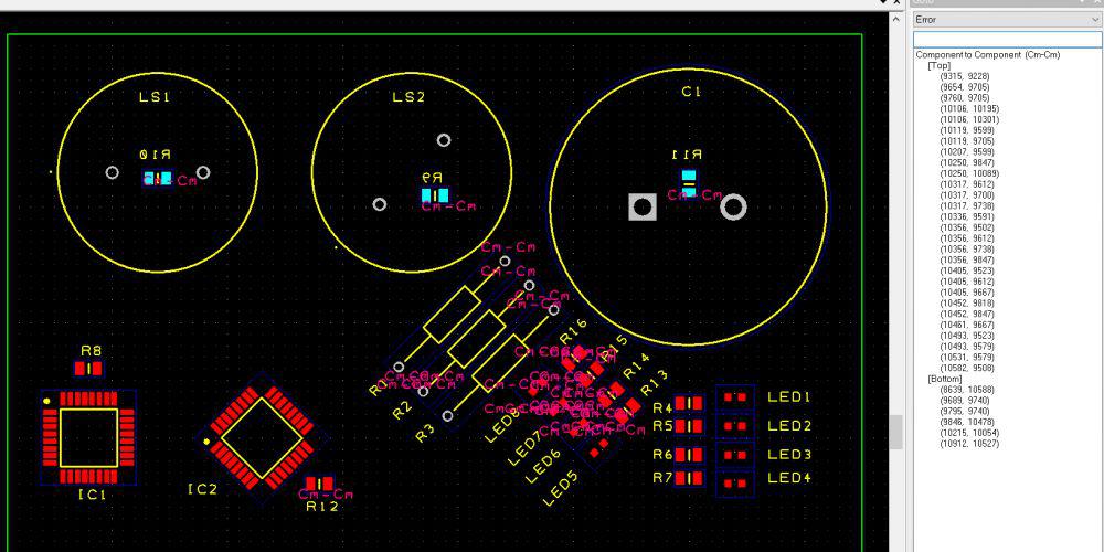
Design Rule Check
Design Rule Check (DRC) is a crucial step in the process of designing a printed circuit board (PCB) in KiCAD. DRC ensures that the PCB design meets the manufacturing constraints and specifications. KiCAD has a built-in DRC tool that checks the design against a set of rules defined by the user.
The DRC tool is located in the “Tools” menu of the PCB editor. The tool checks the design for errors such as overlapping pads, incorrect track width, and clearance violations. The tool also checks for design rule violations such as minimum hole size, minimum track width, and minimum clearance.
KiCAD allows users to define their own design rules. Users can specify the minimum and maximum values for various design parameters such as track width, clearance, drill size, and more. Users can also define rules for specific layers of the PCB.
The DRC tool generates a report that lists all the errors and rule violations in the design. The report includes the location of the error and the type of error. Users can use the report to correct the errors and violations in the design.
In conclusion, the DRC tool in KiCAD is an essential tool for ensuring that the PCB design meets the manufacturing constraints and specifications. Users can define their own design rules and use the DRC tool to check the design for errors and violations. The DRC tool generates a report that helps users correct the errors and violations in the design.
Generating Gerber Files

Once you have finished designing your PCB in KiCad, the next step is to generate Gerber files. These files are used to manufacture the PCB and contain all the necessary information about the board, such as the copper traces, drill holes, and component placements.
To generate Gerber files, go to File > Plot. This will bring up the Plot window. Here, you can select which layers you want to include in the Gerber files. By default, all layers are selected, but you can deselect any layers that you don’t want to include.
Once you have selected the layers, click on the Generate Drill Files button. This will generate the drill files for the PCB. Make sure to select the correct drill file format for your manufacturer.
Next, click on the Generate Gerber Files button. This will generate the Gerber files for the PCB. You can choose to generate a single ZIP file containing all the Gerber files or generate individual files for each layer.
Before generating the Gerber files, make sure to check the settings in the Plot window. You can adjust the plot options to customize the output, such as the line width, aperture sizes, and scaling.
After generating the Gerber files, it’s important to double-check them to ensure that everything looks correct. You can use a Gerber viewer to view the files and check for any errors or issues.
In conclusion, generating Gerber files in KiCad is a straightforward process that requires a few clicks. By following the steps outlined above, you can ensure that your PCB is ready for manufacturing.
Conclusion

In conclusion, KiCad is a powerful open-source tool for designing electronic circuits and printed circuit boards. Its intuitive interface and extensive library of parts make it easy for users of all skill levels to create professional-quality schematics and PCB layouts.
One of the biggest advantages of KiCad is its active community of users and developers. This means that there is a wealth of resources available online, including tutorials, forums, and libraries of pre-made parts. Additionally, KiCad’s open-source license allows users to modify and customize the software to suit their specific needs.
While KiCad may have a steeper learning curve than some other PCB design tools, the effort is well worth it for those who are serious about designing high-quality circuits. With its powerful features and flexibility, KiCad is an excellent choice for hobbyists, students, and professionals alike.
Overall, KiCad is a reliable, versatile, and cost-effective solution for designing electronic circuits and PCBs. Whether you are just starting out or looking to upgrade your current design tools, KiCad is definitely worth considering.
