Silkscreen Altium is a popular technique used in the electronics industry to label and mark printed circuit boards (PCBs). Silkscreen printing is a process that involves applying a layer of ink onto the PCB surface through a stencil. This technique allows manufacturers to add text, graphics, and symbols to the PCB, making it easier to identify components and trace connections.
Silkscreen Altium is an essential step in the PCB manufacturing process. It is used to provide visual cues to help technicians and engineers identify components and trace connections. The silkscreen layer is typically applied after the solder mask layer, which protects the copper traces from oxidation and contamination. Silkscreen printing can be done using a variety of colors, making it easy to differentiate between different components and signals.
Silkscreen in Altium
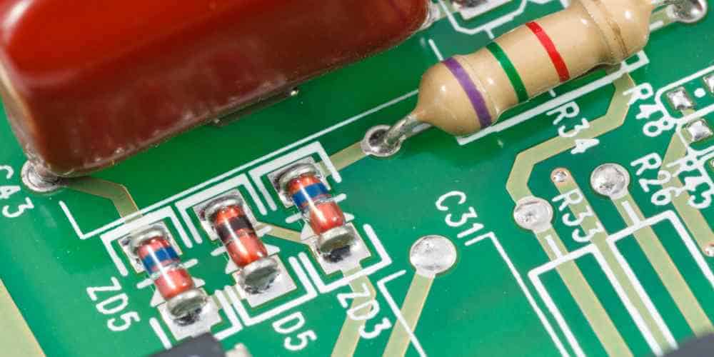
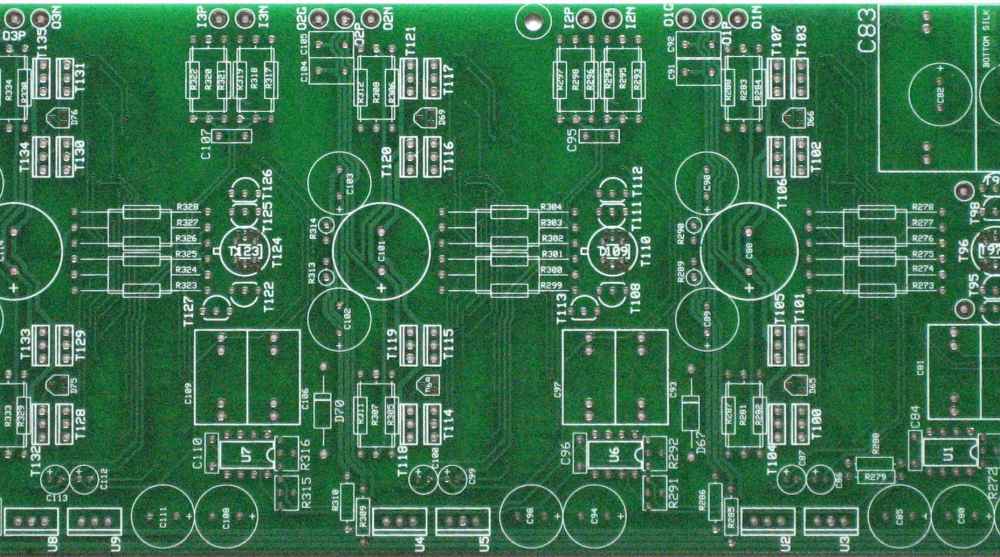
Silkscreen is a layer in Altium that is used to add graphical information to the surface of a PCB. It is used to identify the components, their values, and positions on the board. Silkscreen can also be used to add logos, warnings, and other information to the PCB.
In Altium, silkscreen is added to the top and bottom layers of the PCB. The top silkscreen layer is used to identify the components and their values, while the bottom silkscreen layer is used to add any additional information that may be required.
Silkscreen can be added to the PCB by using the Place » Text command in Altium. The text can be added in various fonts, sizes, and colors. Additionally, it is possible to add graphical elements such as lines, circles, and rectangles to the silkscreen layer.
It is important to note that silkscreen should not be used to add any information that is critical to the functionality of the PCB. Silkscreen is purely for informational purposes and should not be relied upon for any critical information.
In conclusion, silkscreen in Altium is a useful tool for adding graphical information to the surface of a PCB. It can be used to identify components, their values, and positions on the board. However, it should not be used for any critical information and should be used only for informational purposes.
Creating a Silkscreen Layer in Altium
Silkscreen layer is an essential element of any PCB design. It provides clear and comprehensive information about the components, their placement, and orientation, which helps in the assembly and manufacturing process. In Altium, creating a silkscreen layer is a straightforward process that can be accomplished in a few simple steps.
To create a silkscreen layer in Altium, follow these steps:
- Open your PCB design project in Altium.
- Navigate to the PCB Layout editor.
- Click on the ‘Layer Stack Manager’ button in the top toolbar.
- In the Layer Stack Manager dialog box, click on the ‘Add Layer’ button.
- Select the ‘Silkscreen’ option from the list of available layers.
- Choose the appropriate color and name for the silkscreen layer.
- Click on the ‘OK’ button to add the silkscreen layer to your design.
Once you have added the silkscreen layer to your design, you can start adding silkscreen objects to it. These objects can include component outlines, reference designators, pin numbers, logos, and other relevant information. To add a silkscreen object, select the ‘Silkscreen’ layer from the layer drop-down menu, and use the appropriate drawing tools to create the object.
It is essential to ensure that the silkscreen objects are legible and clearly visible on the PCB. You can adjust the size, font, and color of the silkscreen objects to make them more visible. Altium also provides a range of tools and features that can help you align and position the silkscreen objects accurately.
In conclusion, creating a silkscreen layer in Altium is a simple and straightforward process. By following the steps outlined above, you can easily add a silkscreen layer to your PCB design and start adding silkscreen objects to it. With the right tools and techniques, you can create a clear and comprehensive silkscreen layer that will help in the assembly and manufacturing process.
Placing Silkscreen Objects in Altium

Silkscreen is a critical component of any PCB design. It is the layer that provides the visual representation of the board’s component placement, orientation, and polarity. In Altium, placing silkscreen objects is a straightforward process that can be completed in a few simple steps.
To place a silkscreen object in Altium, follow these steps:
- Open the PCB document in Altium.
- Select the Silkscreen layer from the layer drop-down menu.
- Click on the Place » Text or Place » Graphics option from the toolbar.
- Choose the desired silkscreen object from the list of available options.
- Click on the location where you want to place the object on the board.
- Adjust the size, orientation, and other properties of the object as needed.
Altium provides a wide range of silkscreen objects that can be used to convey various information about the board’s components. Some of the most commonly used silkscreen objects include reference designators, component outlines, logos, and text labels.
When placing silkscreen objects in Altium, it is essential to ensure that they are not placed too close to other components or traces on the board. This can cause clearance issues and ultimately lead to manufacturing errors. It is also crucial to use clear and concise labeling to avoid confusion during assembly and testing.
In conclusion, placing silkscreen objects in Altium is a simple and straightforward process that can be completed in just a few steps. By following the best practices and guidelines for silkscreen placement, designers can ensure that their PCB designs are accurate, clear, and easy to manufacture.
Editing Silkscreen Objects in Altium
Silkscreen objects are graphics or text that are printed on the surface of a printed circuit board (PCB) to provide visual information about the board’s components, orientation, and other details. In Altium, you can easily edit silkscreen objects to customize their appearance and content.
To edit a silkscreen object in Altium, follow these steps:
- Open the PCB design file in Altium.
- Select the silkscreen object you want to edit by clicking on it.
- Right-click on the selected object and choose “Properties” from the context menu.
- In the Properties panel, you can change various attributes of the silkscreen object, such as its position, size, rotation, font, color, and layer.
- To edit the text content of a silkscreen object, double-click on it to enter text editing mode. You can then type in new text, change the font and size, and apply formatting such as bold, italic, or underline.
- To add a new silkscreen object, select the “Place » Silkscreen” command from the toolbar or context menu. You can then draw a new object using the available tools, such as line, rectangle, circle, or text.
It is important to note that silkscreen objects should not overlap with other components or traces on the PCB, as this can cause manufacturing errors or electrical issues. Therefore, it is recommended to use the Design Rule Checker (DRC) feature in Altium to check for any violations of design rules related to silkscreen objects.
In summary, Altium provides a user-friendly interface for editing silkscreen objects on PCBs, allowing designers to customize the appearance and content of these important visual elements. By following the above steps and adhering to design rules, designers can ensure a high-quality and reliable PCB design.
Generating Silkscreen Output Files in Altium
Silkscreen is an essential part of the PCB design process, as it provides visual guidance for the assembly and manufacturing of the board. In Altium, generating silkscreen output files is a straightforward process that can be done in just a few steps.
To generate silkscreen output files in Altium, follow these steps:
- Open your PCB design in Altium and go to the Outputs tab in the Project panel.
- Click on Manufacturing Outputs and select Gerber Files.
- In the Gerber Setup dialog box, select the layers you want to include in the silkscreen output files. Make sure to select the SilkS layer.
- Set the output directory and file name for the silkscreen output files.
- Click on OK to generate the silkscreen output files.
It’s important to note that the silkscreen layer should only contain the elements that need to be printed on the board, such as component outlines, reference designators, and logos. It should not include any copper traces or pads.
In addition to generating silkscreen output files, Altium also allows you to preview the silkscreen layer in 3D mode. This can be useful for verifying the placement and alignment of components on the board.
Overall, generating silkscreen output files in Altium is a simple process that can be done quickly and easily. By following these steps, you can ensure that your PCB design includes accurate and clear silkscreen markings for the assembly and manufacturing process.
Best Practices for Silkscreen in Altium
Silkscreen is an essential part of designing printed circuit boards (PCBs) in Altium. It helps to identify components, reference designators, and other important information on the PCB. Here are some best practices for silkscreen in Altium:
Use Clear and Readable Fonts
The font used for silkscreen should be clear and easy to read. Using fancy or decorative fonts can make it difficult to read the text, especially when the PCB is small. Arial, Helvetica, and Verdana are some of the recommended fonts for silkscreen.
Keep Silkscreen Away from Pads and Traces
Silkscreen should be kept away from pads and traces to avoid any interference with the electrical connections. If silkscreen is placed too close to the pads or traces, it can create a short circuit or affect the performance of the PCB. It is recommended to keep a minimum distance of 0.5mm between silkscreen and pads/traces.
Use Consistent and Standardized Designators
Reference designators should be consistent and follow a standardized format throughout the PCB. This helps to avoid confusion and errors during assembly and testing. The designators should be placed close to the component and aligned in a readable orientation.
Use Colors to Differentiate Components
Using different colors for silkscreen can help to differentiate between components and make it easier to identify them. For example, using red for power components, blue for signal components, and green for ground components can help to quickly identify them on the PCB.
Check for Clashes with Mechanical Parts
Silkscreen should be checked for any clashes with mechanical parts like connectors, switches, and buttons. If silkscreen is placed too close to these parts, it can get damaged or peeled off during assembly or use. It is recommended to keep a minimum distance of 1mm between silkscreen and mechanical parts.
By following these best practices for silkscreen in Altium, you can ensure that your PCB is designed with clear and readable silkscreen that is easy to understand and use.
