Are you an electronic student who wishes to make your own printed circuit board due to such factors as competition or inadequate finances? Or, are you a PCB enthusiast who wishes to build on your electronic skills and experience? Assembling a printed circuit board by yourself is pretty fun. If you are a beginner in electronics, it may take you less than a day to manufacture your PCB, a method known as DIY PCB assembly.
DIY printed circuit boards are a PCB type that involves taking your raw materials and assembling the circuit board at your home. In addition, you are not required to contact any manufacturer for assistance in the entire process, and you do everything on your own in case. Here, the success of the procedure depends on your skills. The more skilled you are, the more accurate and productive you will be. You later test your PCBs’ functionality after completing the assembly process. The following information explains the DIY PCB manufacturing process.
DIY PCB Manufacture Process
Manufacturing a DIY printed circuit board involves the following four main iterations:
- Designing
- Preparing the materials
- Producing
- Testing
Designing
Designing the printed circuit board involves selecting the PCB design software suitable for you. A wide range of design software is available, such as KiCad, Altium, etc. In this case, you must consider the complexity of the software. If you are a beginner, please consider an easy-to-use basic entry-level design software. The best software should offer a comprehensive service such as designing, simulation, PCB drawing, editing, signal analysis, and assessing the design output. In addition, the designing software should help you with such functions as designing the schematic, designing the actual PCB, developing the FPGA, developing the embedded structure, 3D PCB viewing, etc.
Furthermore, the latest design software provides a solid solution for designing Single, double, four, and six-layer printed circuit boards. Moreover, you can also consider several other design software such as Cadence, PADS, and Allegro. You can proceed to the actual production work after successfully obtaining your design.
Preparing the Materials
Before kicking off the production process, you may need to prepare some materials. The electronic components will depend on the design of your DIY PCB. In addition, you will require such materials as:
- CCL (Copper Clad Laminate)-Nowadays, you can make your PCB by processing it on the CCL.
- Acetone-During production, you will require acetone to remove any carbon traces on the CCL.
- Thermal transfer paper– the production process will involve using a special thermal transfer ink to print specific patterns on a special paper before transferring them to the product via pressure and temperature.
- Sandpaper-The sandpaper is for polishing the copper-clad laminate’s surface.
- Iron Chloride (FeCl3)-Iron chloride removes any excess copper layer on the CCL board.
- Electric drill- You will also require an electric drill to accurately make
holes on the CCL.
In addition, you will also require other auxiliary equipment such as brushes, laser printers, beakers, irons, tweezers, etc.

Production
DIY PCB production is a lengthy process divided into progressive iterations. The following are the steps to follow during the actual production process:
· Stencil Printing
In this step, you will employ a laser printer to make a drawing of the design on the special thermal transfer paper. You will therefore have a black and white circuit diagram.
· Cutting
You will also need to ensure that the CCL is equal in size to the circuit diagram. Note that this will also be the final product’s size. If the dimensions do not match, cut the CCL to the desired size.
· Polishing
You can smoothen the Copper Clad Laminate surface using sandpaper. Consequently, the final printed circuit board will be smooth and have better quality.
· Transferring
Now transfer the printed circuit diagram to the copper-clad laminate (CCL). You will then need to close the circuit diagram to the copper-clad laminate and press it as you heat. In this case, you can employ an iron box, which is equally effective and easier to get. However, using the iron box, it may take 10 minutes to trace the circuit drawing on the copper-clad laminate ultimately. After completing the transferring process, remove the circuit diagram, and you will have your circuit diagram on the CCL. At this stage, the CCL is purely conductive. Removing the unnecessary copper outside the copper-clad laminate’s surface makes it a pure insulator.
· Removing the copper
In this stage, dip the processed copper-clad laminate into the iron chloride solution to remove any excess copper outside the circuit. In this case, there is no reaction between the iron chloride solution and the carbon in the circuit.
· Decarbonization
Decarbonization removes all the toner transferred on the copper-clad laminate. However, in case your PCB does not have high specifications, you can let the carbon remain. To remove carbon from your PCB, dip it in the acetone solution and then use a soft brush to scrub off the toner gently. In addition, you can also use sandpaper to remove the toner from the CCL surface.
· Drilling
You will need to correctly drill the through holes to install your components on the board. However, this requires predetermining the holes’ positions and then carefully drilling using an electric drill.
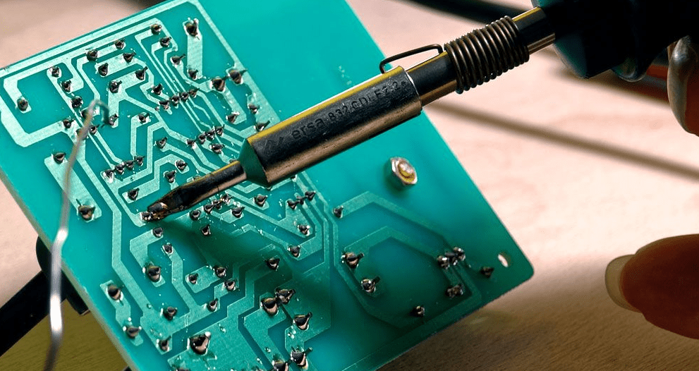
· Assembly
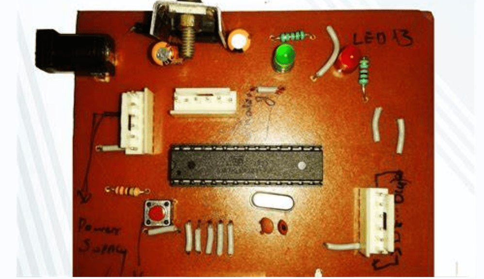
Now, carefully install your electronic components on the board and firmly solder them on the backside.
Testing
Having carried out all the above steps, you now need to test your DIY PCB and determine whether it works as you intended. In addition, this will also tell you whether your DIY PCB is in good condition. In this case, you must close the power switch and check for damages. If there are no component damages, your circuit is okay; therefore, you are good to go.
Conclusion
From the above details, it is possible to fabricate your printed circuit board without contacting any manufacturer. You will therefore have a chance to utilize your skills in electronics. In addition, this method is cheaper compared to getting it done by a large-scale manufacturer. Consequently, you will end up familiarizing yourself with electronic circuits even more. The most substantial advantage of DIY PCB manufacturing is that you can perform the whole process quickly and obtain your intended PCB within a short time.
However, DIY PCB assembly has some disadvantages. For instance, the assembly process is tedious and may not be very efficient as a result. Secondly, you are not guaranteed excellent PCB quality using this method. Thirdly, this manufacturing process is not appropriate for mass PCB production. Finally, it may be difficult for an average person to access all the required materials.
