Table of Contents
ToggleSolar energy has become an increasingly popular source of renewable energy, and solar inverters play a crucial role in converting the direct current (DC) generated by solar panels into usable alternating current (AC) electricity. The printed circuit board (PCB) layout of a solar inverter is a critical aspect of its design, as it affects the overall performance and efficiency of the inverter.
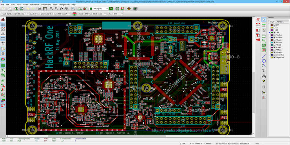
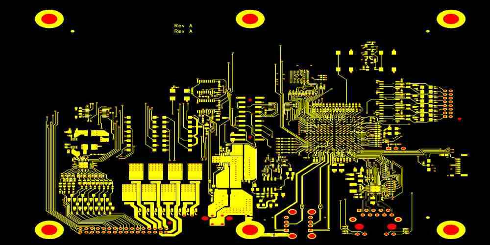
The PCB layout of a solar inverter involves the placement and routing of components on the board to minimize noise and optimize the flow of current. It is essential to ensure that the layout is designed to handle the high voltages and currents involved in solar energy systems. Properly designed PCB layouts can improve the efficiency and reliability of the inverter, reducing the risk of failure and improving the overall performance of the solar energy system.

Solar Inverter PCB Layout Basics
PCB Layout Design Considerations
When designing a solar inverter PCB layout, there are several considerations to keep in mind. These include the size and shape of the PCB, the location of components, and the routing of traces. It is important to ensure that the PCB is designed to fit within the inverter housing and that there is enough space for all components to be placed in the correct locations.
Schematic Design and Component Placement
Before designing the PCB layout, it is important to create a schematic that accurately represents the circuit. The schematic should include all components, their values, and their connections. Once the schematic is complete, the components can be placed on the PCB layout. It is important to place components in a logical and organized manner to ensure that the PCB is easy to assemble and maintain.
Grounding Techniques
Proper grounding is critical for the performance and safety of a solar inverter. Grounding should be done in a way that minimizes noise and interference and ensures that the inverter is safe to operate. There are several grounding techniques that can be used, including star grounding and ground planes.
Routing Guidelines
When routing traces on a solar inverter PCB, it is important to follow certain guidelines to ensure proper performance. Traces should be as short as possible to minimize resistance and capacitance. High current traces should be wider to minimize resistance and heat. It is also important to keep signal traces away from high current traces to minimize noise and interference.
In summary, designing a solar inverter PCB layout requires careful consideration of several factors, including PCB layout design, schematic design and component placement, grounding techniques, and routing guidelines. By following these guidelines, a high-quality and reliable solar inverter can be designed.
Advanced Techniques for Solar Inverter PCB Layout

High-Speed Design Techniques
When designing a solar inverter PCB, high-speed design techniques are crucial to ensure optimal performance. Here are some advanced techniques to consider:
- Use controlled impedance routing to minimize signal reflections and ensure signal integrity.
- Place decoupling capacitors close to the power pins of ICs to reduce noise and voltage fluctuations.
- Use differential pairs for high-speed signals to reduce electromagnetic interference (EMI).
- Minimize the length of high-speed traces to reduce signal delay and improve timing.
EMC Considerations
Electromagnetic compatibility (EMC) is critical in solar inverter PCB layout to ensure that the device operates reliably and does not interfere with other electronic devices. Here are some EMC considerations to keep in mind:
- Use shielding to reduce EMI and prevent interference with other electronic devices.
- Place high-frequency components away from sensitive circuits to reduce noise coupling.
- Use ground planes to reduce ground loops and improve signal integrity.
- Ensure that the PCB layout complies with EMC regulations and standards.
Thermal Management
Thermal management is essential in solar inverter PCB layout to prevent overheating and ensure optimal performance. Here are some advanced techniques to consider:
- Use thermal vias to dissipate heat from power components and reduce thermal resistance.
- Place power components away from sensitive circuits to reduce heat dissipation and prevent thermal runaway.
- Use heat sinks and fans to improve heat dissipation and reduce the operating temperature of the PCB.
- Ensure that the PCB layout complies with thermal regulations and standards.
By implementing these advanced techniques in solar inverter PCB layout, you can ensure optimal performance, reliability, and compliance with regulatory standards.
Testing and Validation of Solar Inverter PCB Layouts

Testing and validation are crucial steps in ensuring that a solar inverter PCB layout is functional and reliable. Here are some of the common testing and validation techniques used in the industry:
1. Component Testing
Before assembling the PCB, it is important to test each component to ensure that it is functioning correctly. This includes testing resistors, capacitors, diodes, transistors, and other components for their specified values and tolerances.
2. Power-On Testing
Once the PCB is assembled, it is time for power-on testing. This involves verifying that the power supply is delivering the correct voltage and that the inverter is producing the expected output waveform. It is important to check for any abnormal heat or noise during this testing phase.
3. Load Testing
After the power-on testing, the inverter should be tested under load conditions. This involves connecting the inverter to a load and monitoring its performance. Load testing can reveal any issues with the inverter’s stability, efficiency, or output waveform.
4. Environmental Testing
Environmental testing involves subjecting the solar inverter to various environmental conditions such as temperature, humidity, and vibration. This testing ensures that the inverter can operate reliably in different conditions.
5. Safety Testing
Safety testing is essential to ensure that the solar inverter meets safety standards and regulations. This includes testing for electrical safety, fire safety, and electromagnetic compatibility.
In conclusion, testing and validation are critical steps in ensuring that a solar inverter PCB layout is reliable and safe. By following these testing techniques, manufacturers can produce high-quality solar inverters that meet the needs of their customers.

