Web PCB design is an essential part of the electronics industry. PCB (Printed Circuit Board) design is the process of creating a layout for the components and connections on a printed circuit board. It is the backbone of any electronic device, as it connects the different components and ensures their proper functioning.
Web PCB design has revolutionized the way we design and manufacture printed circuit boards. It has made the process faster, more efficient, and more accessible to a wider audience. With the advent of cloud-based design tools, designers can now collaborate on PCB designs from anywhere in the world, making it easier to bring new products to market. Additionally, web PCB design tools offer features such as design rule checking, real-time collaboration, and automatic routing, making it easier to create complex designs with minimal errors.
Basics of Web PCB Design
Web PCB design is the process of creating printed circuit boards (PCBs) for use in web applications. PCBs are boards that contain electrical components and conductive pathways that allow for the flow of electricity. In web applications, PCBs are used to control various aspects of the application, such as user input, data processing, and data storage.
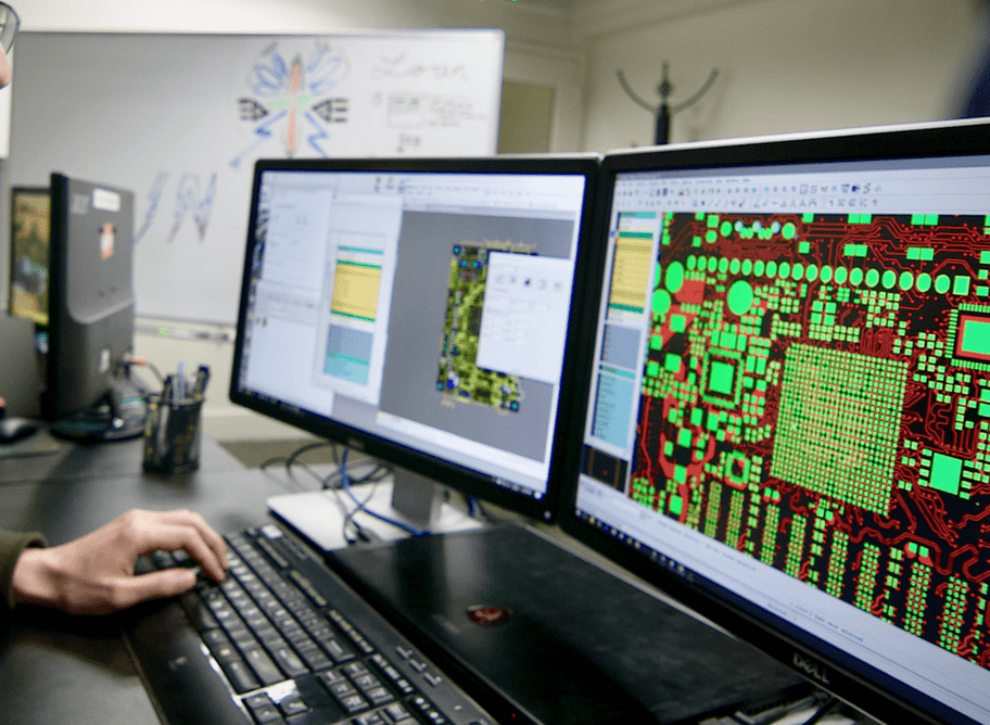
The design of a web PCB involves several key steps. First, the designer must determine the overall size and shape of the board, as well as the location of the various components. This is typically done using specialized software that allows for the creation of a virtual prototype of the board.
Once the basic layout of the board has been determined, the designer must then select the appropriate components for the board. This involves selecting components that are compatible with the board’s size and shape, as well as components that are appropriate for the intended use of the board.
After the components have been selected, the designer must then create a schematic diagram of the board. This diagram shows the connections between the various components and allows the designer to ensure that the board will function as intended.
Finally, the designer must create the physical layout of the board. This involves placing the components on the board and routing the conductive pathways between them. The designer must also ensure that the board meets any necessary safety and regulatory requirements.
Overall, the design of a web PCB is a complex process that requires a great deal of skill and expertise. However, with the right tools and knowledge, it is possible to create high-quality PCBs that are perfectly suited for web applications.
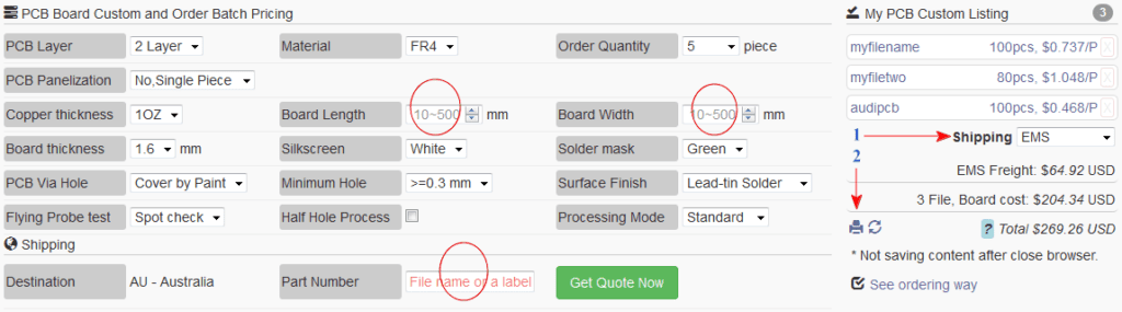
Tools and Software for Web PCB Design

When it comes to web PCB design, there are a variety of tools and software available to help you create high-quality circuit boards. Here are a few examples:
1. Eagle PCB Design Software
Eagle PCB Design Software is a popular choice for PCB design. It is user-friendly and offers a wide range of features, including schematic capture, board layout, and autorouting. Eagle also has a large community of users who share tips and tricks, making it easy to find help when you need it.
2. Altium Designer
Altium Designer is a powerful PCB design software that offers advanced features for professional designers. It includes schematic capture, board layout, and 3D visualization, as well as tools for simulation and design verification. Altium Designer also has a large library of components and templates, making it easy to get started on your project.
3. KiCAD
KiCAD is a free, open-source PCB design software that is gaining popularity among designers. It includes schematic capture, board layout, and 3D visualization, as well as tools for design verification and simulation. KiCAD also has a large library of components and templates, and its open-source nature means that users can customize it to their specific needs.
4. CircuitMaker
CircuitMaker is a free, community-driven PCB design software that offers a range of features for both beginners and advanced users. It includes schematic capture, board layout, and 3D visualization, as well as tools for design verification and simulation. CircuitMaker also has a large library of components and templates, and its community of users provides support and guidance.
Overall, the choice of PCB design software will depend on your specific needs and budget. It’s important to do your research and choose a software that fits your requirements and skill level.
Design Considerations for Web PCBs
When designing printed circuit boards (PCBs) for web applications, there are several key considerations to keep in mind. Here are some important factors to consider:
1. Size and Shape
Web PCBs are often smaller and more compact than traditional PCBs, so size and shape are critical considerations. The PCB must fit into the web application without interfering with other components or taking up too much space.
2. Power Consumption
Web PCBs must be designed to minimize power consumption. This is especially important for battery-powered devices, as excessive power consumption can quickly drain the battery and reduce the device’s lifespan.
3. Environmental Factors
Web PCBs are often exposed to harsh environmental conditions, such as extreme temperatures, humidity, and dust. It is important to design the PCB with these factors in mind to ensure that it can withstand these conditions without malfunctioning.
4. Connectivity
Web PCBs often require connectivity to other devices or networks. It is important to design the PCB with the appropriate connectivity options, such as Wi-Fi, Bluetooth, or cellular, depending on the specific application requirements.
5. Cost and Manufacturing
Finally, cost and manufacturing considerations are critical when designing web PCBs. The PCB must be designed with cost-effective materials and manufacturing processes to ensure that it can be produced at scale without breaking the bank.
In summary, designing PCBs for web applications requires careful consideration of size, power consumption, environmental factors, connectivity, and cost. By keeping these factors in mind, designers can create high-quality web PCBs that meet the specific needs of their applications.
Testing and Debugging Web PCBs
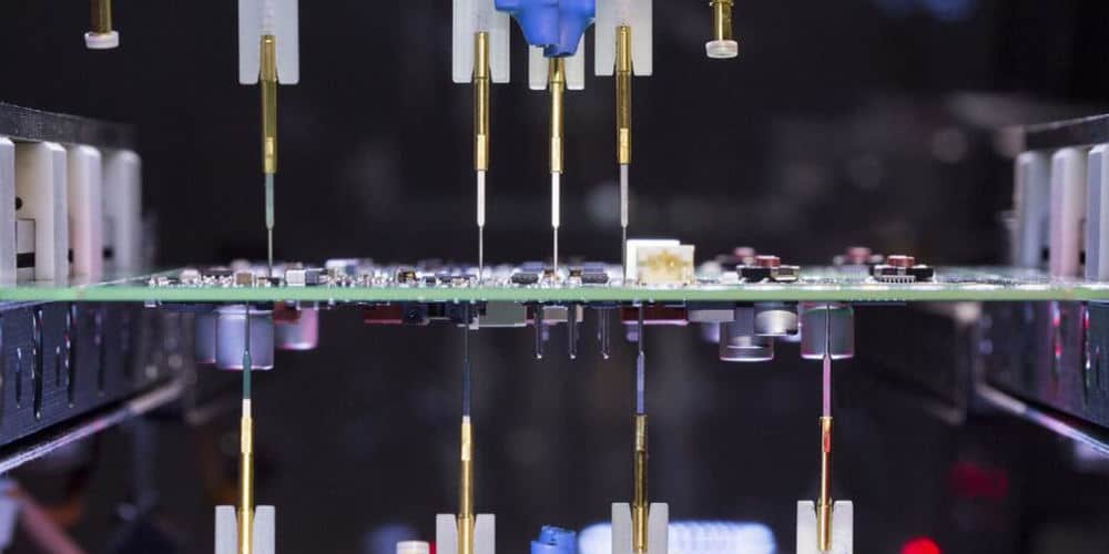
Once your web PCB design is complete, it’s time to test and debug it to ensure that it works as expected. Here are some tips to help you with this process:
1. Visual Inspection
Start by performing a visual inspection of your PCB. Look for any obvious errors, such as missing components, incorrect polarity, or solder bridges. Check that all the components are in the correct location and orientation. Ensure that there are no physical defects such as cracks or scratches on the PCB.
2. Power Up
Next, power up your PCB and check that it is receiving power correctly. Use a multimeter to measure the voltage at various points on the board to ensure that it is within the expected range. Check that the power supply is stable and that there are no voltage drops.
3. Functional Testing
Once you have verified the power supply, move on to functional testing. This involves testing each component and circuit on the PCB to ensure that it is working as expected. Use a signal generator and oscilloscope to test the signals at various points on the board. Check that the signals are within the expected range and that they are not distorted.
4. Software Testing
If your web PCB includes a microcontroller or other programmable device, you will need to test the software as well. Use a debugger or emulator to step through the code and ensure that it is working correctly. Test all the functions and features of the software to ensure that they are working as expected.
5. Environmental Testing
Finally, perform environmental testing to ensure that your web PCB can withstand the conditions it will be exposed to. Test your PCB under various temperature and humidity conditions to ensure that it can operate reliably in different environments.
By following these steps, you can ensure that your web PCB is working correctly and is ready for deployment. Remember to document your testing process and results to help you with future troubleshooting if necessary.
