Table of Contents
ToggleA four-layer PCB layout is a type of printed circuit board that is used to connect electronic components. It consists of four layers of conductive material, with insulating layers in between them. These layers are stacked on top of each other to create a compact and efficient circuit board.
The four-layer PCB layout is widely used in the electronics industry due to its ability to handle complex circuits. It allows for a greater number of components to be placed on the board, which can lead to a reduction in size and weight of the final product. The four-layer design also provides better signal integrity, as the ground and power planes can be isolated from the signal traces. This results in less noise and interference, leading to improved performance.

Basics
What is a 4 layer PCB layout?
A 4 layer PCB layout is a printed circuit board design that consists of four layers of conductive material separated by insulating layers. The layers are interconnected by plated-through holes, which allow signals to pass between the layers. The four layers typically consist of two signal layers, one power plane, and one ground plane.
Why use a 4 layer PCB layout?
A 4 layer PCB layout is used when the design requires more complex routing of signals and power. It provides additional layers for routing signals, which reduces the amount of crosstalk between signals and increases the signal integrity. The power and ground planes provide a low impedance path for the current, which helps to reduce the noise in the system.
Design considerations for 4 layer PCB layouts
When designing a 4 layer PCB layout, there are several considerations to keep in mind. The following are some of the key design considerations:
- Signal routing: The signal routing should be done in a way that minimizes the length of the traces and reduces the amount of crosstalk between signals.
- Power and ground planes: The power and ground planes should be placed close to each other to reduce the loop area and provide a low impedance path for the current.
- Via placement: The vias should be placed in a way that minimizes the impedance of the signal path and reduces the crosstalk between signals.
- Component placement: The components should be placed in a way that minimizes the length of the traces and reduces the amount of crosstalk between signals.
In summary, a 4 layer PCB layout is used when the design requires more complex routing of signals and power. It provides additional layers for routing signals, which reduces the amount of crosstalk between signals and increases the signal integrity. When designing a 4 layer PCB layout, several considerations need to be kept in mind, such as signal routing, power and ground planes, via placement, and component placement.
Design Process

When designing a 4 layer PCB layout, there are several steps that need to be followed to ensure a successful outcome. These steps include schematic capture, component placement, routing, and the creation of ground and power planes.
Schematic Capture
The first step in the design process is to capture the schematic of the circuit that will be implemented on the PCB. This schematic will serve as a reference for the entire design process and will be used to create the physical layout of the PCB.
Component Placement
Once the schematic has been captured, the next step is to place the components on the PCB. Component placement is critical to the success of the design, as it will dictate the routing of the traces on the PCB. Components should be placed in a logical and organized manner, taking into consideration factors such as signal integrity, thermal management, and ease of assembly.
Routing
After the components have been placed, the next step is to route the traces on the PCB. This involves connecting the various components on the PCB using copper traces. The routing process should be done in a way that minimizes noise and interference, while also ensuring that the PCB is compact and efficient.
Ground and Power Planes
Finally, the ground and power planes must be created. These planes provide a low-impedance path for the return currents and help to reduce noise and interference. The ground plane should cover as much of the PCB as possible, while the power plane should be placed adjacent to the ground plane.
By following these steps, a successful 4 layer PCB layout can be designed and implemented.
Manufacturing

Gerber files and CAM data
Gerber files and computer-aided manufacturing (CAM) data are essential for producing a four-layer PCB layout. The Gerber files contain the information needed to create the copper traces, solder mask, and silkscreen layers. The CAM data is used to generate the drill files, which are used to create the holes for the vias and through-hole components.
Before sending the files to the manufacturer, it’s important to verify that they are correct. This can be done using a Gerber viewer or CAM tool. It’s also important to ensure that the manufacturer can work with the specific software used to create the files.
Stackup and layer stack management
The stackup and layer stack management are critical aspects of four-layer PCB layout manufacturing. The stackup defines the order and thickness of each layer, and the layer stack management ensures that the layers are aligned correctly.
The stackup should be designed to meet the specific requirements of the PCB, such as impedance control or heat dissipation. The layer stack management should be checked using a cross-sectional view to ensure that the layers are aligned correctly.
Drilling and plating
Drilling and plating are the processes used to create the vias and through-hole components. The manufacturer will use the drill files to create the holes, and then plate them with copper to create the electrical connections.
It’s important to ensure that the drill files are accurate and that the manufacturer can produce the required hole sizes. The plating process should also be monitored to ensure that the copper is deposited evenly and that the vias are properly connected.
Testing and inspection
Testing and inspection are crucial to ensuring that the finished four-layer PCB layout meets the required specifications. The manufacturer should perform electrical testing to verify that the connections are correct and that there are no shorts or open circuits.
Visual inspection should also be performed to check for any defects, such as scratches or delamination. The finished PCB should be inspected using a microscope to ensure that the solder mask and silkscreen layers are aligned correctly.
Overall, the manufacturing process for a four-layer PCB layout requires careful attention to detail and strict quality control. By following these guidelines, you can ensure that your PCB meets the required specifications and functions properly.
Advanced Techniques
Impedance Control
Impedance control is a critical aspect of designing a 4 layer PCB layout. It ensures that the signal integrity is maintained throughout the board. Advanced techniques can be used to achieve precise impedance control. Some of the techniques include:
- Controlled dielectric constant materials
- Controlled trace width and spacing
- Controlled trace thickness
- Controlled via placement
EMI/EMC Considerations
EMI/EMC considerations are crucial in high-frequency applications. Advanced techniques can be used to minimize EMI/EMC issues. Some of the techniques include:
- Ground planes and power planes
- Shielding and filtering
- Controlled impedance routing
- Isolation techniques
Blind and Buried Vias
Blind and buried vias are used to save space on the PCB and to reduce the number of layers required. Advanced techniques can be used to implement blind and buried vias. Some of the techniques include:
- Laser drilling
- Sequential lamination
- Stacked vias
- Via-in-pad
Microvias
Microvias are used to connect the outer layers of the PCB to the inner layers. Advanced techniques can be used to implement microvias. Some of the techniques include:
- Laser drilling
- Copper filling
- Staggered microvias
- Via-in-pad
In conclusion, advanced techniques can be used to achieve precise impedance control, minimize EMI/EMC issues, implement blind and buried vias, and implement microvias. These techniques are critical in designing a 4 layer PCB layout that meets the requirements of high-frequency applications.
Tools and Resources

PCB design software
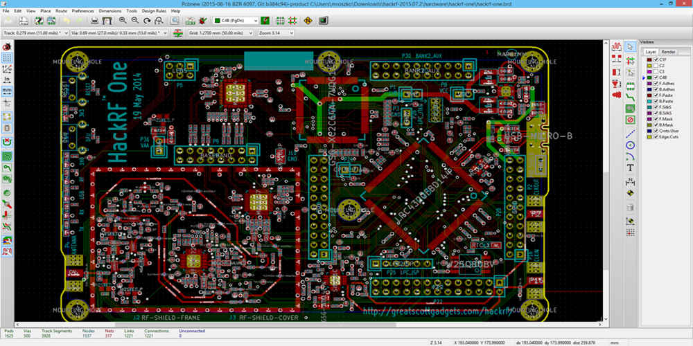
PCB design software is an essential tool for designing and laying out a 4 layer PCB. There are many options available, both paid and free. Some of the most popular PCB design software include Altium Designer, Eagle PCB, KiCAD, and Proteus. Each software has its own strengths and weaknesses, so it’s important to choose the one that best suits your needs and budget.
Simulation and analysis tools
Simulation and analysis tools are important for testing and verifying the design of a 4 layer PCB before it’s manufactured. These tools help to identify potential issues and optimize the design for better performance. Some of the most popular simulation and analysis tools for PCB design include LTSpice, PSpice, and Simulink.
Industry standards and guidelines
There are many industry standards and guidelines that must be followed when designing a 4 layer PCB. These standards ensure that the PCB is safe, reliable, and meets the required specifications. Some of the most important industry standards and guidelines include IPC-2221, IPC-2222, and IPC-7351.
Online communities and resources
There are many online communities and resources available for PCB designers. These resources provide valuable information, tips, and advice on designing and laying out a 4 layer PCB. Some of the most popular online communities and resources include Reddit’s r/PrintedCircuitBoard, Electronics Stack Exchange, and EEVblog.
In conclusion, using the right tools and resources is essential for designing and laying out a 4 layer PCB. By using the right PCB design software, simulation and analysis tools, industry standards and guidelines, and online communities and resources, you can ensure that your PCB is safe, reliable, and meets the required specifications.

