Both basic and advanced electronic gadgets rely on PCBs to function. It is crucial not just because it facilitates electric connections between parts. But it also transmits digital and analog signals, electricity distribution systems, and data transfer extremely high frequency signals.
However, numerous additional requirements should be addressed in printed circuit board design and production with the advent of 5G. To better explain the implications of 5G on PCB design and production, we’ve included some key points below.
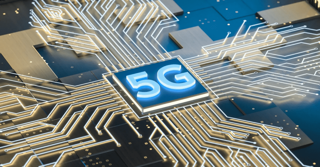
What is 5G?
When it comes to mobile broadband, 5G is the latest generation. And it comes in low-band, high-band, and mid-band variants. This cutting-edge innovation utilizes modular cell sites to transmit encoded data. The encoded data gets transferred over highest operating frequency’s wavelength of radio via wired and wireless networks.
Compared to 4G, the 5G technology offers:
1. Fast speeds digital signals:
Due to its bigger bandwidth, 5G is significantly quicker than prior services. It responds to user queries within just a few seconds. Unlike 4G, which tops out at 1 Gbps, 5G has the potential to reach speeds of up to 20 Gbps.
2. Lower Inactivity:
The current generation of 5G networks, whether sub-6 Gigahertz or mmWave, has better connectivity compared to traditional 4G networks. This enhances the technology’s reliability. This, in turn, improves the customer experience. Besides this, it opens up new fields and uses for technology.
3. Better connectivity and high thermal conductivity:
With 5G’s faster speeds and lower latency, more cloud applications, machine-learning technologies, sensors, and smart devices, can connect to the internet.
4. Greater Coverage electrical connections:
5G’s enhanced cellular-to-Wi-Fi mobility and communication range are two of its most notable benefits. The advent of 5G networks will allow essential industries like healthcare and emergency response to finally have access to the internet in previously inaccessible regions.
5G is distinct from but not a substitute for 4G technology. Most 5G-enabled gadgets still require 4G coverage for the best operation at this time.
Why Is 5g Technology Important For PCB Industry?

The market for 5G PCB layout has shifted due to these advancements in connectivity. With the proliferation of 5G comes a greater need for flexible PCB design. It helps to meet the expanding demands of the industry.
4G PCBs rely on a baseband station, distant wireless unit, antennas, metal wire, and optical fibers. In contrast to 4G PCBs, 5G PCBs feature both decentralized and centralized units. This is in addition to broadband control systems and cellphone cloud technologies. Despite the mixed high speed frequencies, 5G PCBs still need a greater number of base stations. The purpose is to provide the necessary antennas and coverage.
Since 5G will soon touch every part of the manufacturing process. PCB designers, producers, and other professionals in the sector cannot afford to ignore it.
1. Consumer Awareness
PCB makers need to take measures to keep up with the rising and evolving demands of the customer market. It helps users become more conscious of the 5G service. And 5G-enabled gadgets have become more easily available on the market as 5G networks evolve and extend to cover more locations and devices. So, too must the technologies employed to maintain them.
2. Data Traffic
25% of all mobile data usage will be handled by 5G by 2024, according to experts. Thanks to its low latency, speed, adaptability, and reliability. Videos, mobile games, calls, browser history, and app usage are all going to be tracked. PCB makers and product designers must optimize existing procedures. Also, they should build new ones to keep up with the increased data volume. It helps in experiencing any performance issues. Sluggish data transfer or intermittent connectivity are common performance issues.
3. Industrial Applications
Cellphones and other consumer gadgets are where you’re most likely to hear the word “5G”. But, these advancements have allowed 5G to spread into other fields, such as medicine, transportation, production, retail, media, and entertainment. As PCBs become more ubiquitous, so too will the need for PCB producers. Both PCBs and 5G benefit from this expansion since new applications for their technologies, like in agriculture, are made possible.
Major Applications and Benefits of 5G PCB

There are various industries that could benefit from 5G PCBs. The following are some common uses for 5G PCBs:
· Smart houses
Connecting mobile devices like iPads and smartphones to smart home systems is now feasible, thanks to 5G PCBs. Through a wireless network, you can keep tabs on and manage your home’s many functions. Additionally, because of 5G’s lightning-fast speeds, individuals may view live CCTV footage on their smartphones.
· Fast-speed mobile network
Improved communication is one benefit of 5G’s lightning-fast speeds. This is so because voice and text communication become more efficient at higher speeds. Enhanced transmission rates also make making and receiving phone calls and sending several text messages in a short amount of time much simpler and more efficient.
· Logistics and power supply lines
Tracking logistics is made possible with the use of a 5G mobile device connected to a superfast 5G network. It is also useful for online shipment management and delivery using mobile devices.
· Entertainment
Live streaming of your favorite shows is now glitch-free thanks to the lightning-fast 5G network. Netflix videos, for example, may be watched on a 5G printed circuit board smartphone without experiencing severe interruptions. Also, video and film download speeds are very impressive.
· Healthcare Sector
When it pertains to healthcare procedures, 5G in the medical industry is revolutionary. Having real-time footage of an operation can be very useful for both the patient and the surgeons.
How Is 5G Affecting Printed Circuit Board Companies?
In order to maintain pace with the rapid development of 5G technology, PCB makers must use design, PCB materials, procedures, and manufacturing methods that will expand with the technology. Some shifts that need to be considered by PCB manufacturers are:
· Compact Designs:
Consumer gadgets, such as cell phones, wearable health gadgets, and voice assistants, are constantly evolving as companies compete with one another by making novel, daring design decisions. Take, for example, the modern craze for foldable smartphones. In order to accommodate 5G networks, more malleable materials than those used in conventional PCBs will need to be explored. As new trends and features enter the market, devices are getting more efficient and smaller, necessitating compact, lighter boards that do not lose performance.
· Thinner Patterns:
For this reason, many 5G devices call for HDI-printed circuit boards to ensure that no signals are lost. Also, it ensures that no transmissions are slowed down. Subtractive design and other traditional PCB fabrication methods can lead to PCBs with crossed tracks. They further degrade 5G performance. This problem can be solved by employing a semi-additive manufacturing technique. This technique makes more accurate and precise trace lines, allowing for higher circuit densities.
· AOI Systems:

AOIs are used to check printed circuit boards for defects in design. Also, they check both the functionality and conformance to specifications before mass production. Because they demand so little of either the inspector or the time of others, they have a clear advantage over manual analysis. To further conserve materials and space, factories can streamline their AOI operations and use as few devices as possible. For 5G networks, AOI systems will need to be more refined than ever before in order to detect and fix even the tiniest misalignments and pinpoint problems as quickly as possible.
Opportunities & Challenges of 5G Technology
As 5G becomes an increasingly important aspect of PCB production, manufacturers will likely face a number of obstacles and opportunities.
Challenges of 5G PCB Technology
Antenna housing and heat dissipation materials present two major obstacles for 5G PCB layouts:
- Antenna Box – Analog and digital frequencies
As 5G networks will run at extremely higher frequencies (EHF). There is a need for more array antennas and base stations for reliable service. A large antenna array box accommodating these arrays of antennas will need to be designed by PCB manufacturers (AAU).
- Heat management
Better heat management is required from manufacturers as a result of increased speed and power output by 5G high speed cellular network and decreased latency. Structures that dissipate heat and elements with low dielectric constant values are used to prevent PCB failure and eliminate loss of higher signal speeds, respectively.
5G PCB Opportunities
The benefits to customers of modifying PCB layouts to work with 5G technology are obvious. They will receive a device that is faster and more reliable. In addition to this, they get better access to more cutting-edge capabilities. However, there may be some overlap in the advantages of businesses across different types of manufacturing machinery. The biggest advantage comes from satisfying customer demand.
The increasing need for more robust and versatile gadgets and the parts that power them will drive PCB market expansion. The demand for circuit boards (PCBs) is increasing as more consumers and businesses transition to 5G devices.
Manufacturing plants have the resources and systems in place to adjust to technology. This enables them not to fall behind contemporary technology. They will keep growing as trends shift and coverage extends. In addition to satisfying customer demands, they should also offer higher profits.
Final Thoughts
5G now has a permanent place in the information age. It has a long-lasting impact on PCB layout and production. Because of its faster speed, dependability, and improved user experience. PCB manufacturers and designers are making greater investments in cutting-edge technologies. This step ensures to bring their products up to speed.
PCB manufacturers and designers encounter many obstacles when working on 5G boards. But they’ve devised solutions that allow for reliable PCBs. The boards are compatible with the 5G system and make the most of the advantages it provides.
