When it comes to the accuracy, precision, and dependability requirements of the electronics industry, PCB designing services are important. Creating a functioning prototype is the final step in the PCB design phase, which begins with the designing of the electrical systems architecture. Here, we’ll examine the process of PCB designing in further detail. It includes different phases like testing, assembly, fabrication, layout, and design.
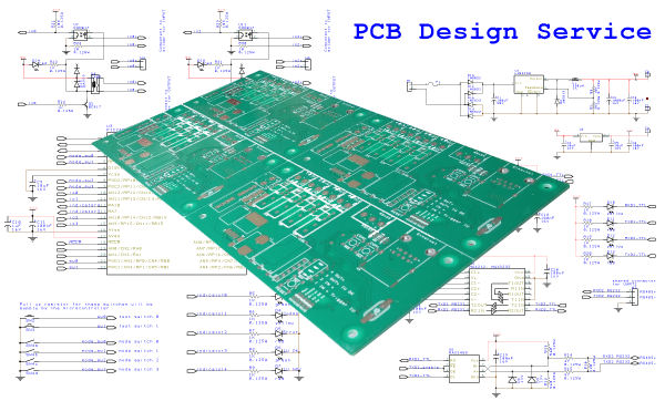
Step-by-Step Guide to Printed Circuit Board Design Services
Here are the nine steps involved in creating a PCB, from sketching to finished files:
1. Understanding electrical parameters in PCB Manufacturing
You should be familiar with the system’s electrical properties before beginning a PCB design.
- Type of Signals
- Detailed schematic and net wiring list
- Location and type of circuit connectors and components
- Considerations in Shielding
- Characteristics of Impedance
- Limitations of Capacitance
- Voltages
- Current maximum magnitudes
2. Create the schematic diagram
The first stage in designing any circuit board should be drawing up a schematic, which is an outline of the board’s intended electrical layout. As of right now, it is not a mechanical depiction.
3. Use Schematic Capture to create PCB layout services
Your PCB supplier should collaborate with your key engineers to create a schematic using a platform like Altium, Allegro, or Mentor PADS® that will detail the functionality and placement of your board’s elements. You’ll need to have a mechanical engineer load your schematic into their gadget of choice to see how it all fits together.
4. Designing PCB stack up
Due to impedance, the rate and magnitude of electricity flow along a trace needs consideration at an initial stage in PCB designing. When mechanical engineer gets tasked with designing and fitting a PCB into a system, they’ll need to know the stack up so they can do it effectively.
5. Defining design rules on PCB board

The IPC, a trade group for electronics and PCB manufacturers, sets the standards and acceptance criteria that must be met at this stage. Everything you want to know about PCB fabrication is present in these guidelines. Finding a PCB design service that is well-versed in IPC regulations is crucial if you wish to prevent extensive alterations and setbacks to your project.
6. Placing components in PCB design process
When it concerns the arrangement of parts on a PCB, layout and design requirements are typically discussed between the PCB provider and the customer. Some components may get prohibited from getting installed in close proximity to one another due to electrical interference requirements. Data sheets for each component (often connections) will be compiled by the PCB vendor and included in the mechanical design for client review.
7. Inserting drill holes
The connection and component parts enable this procedure. About 50% of all flex circuits sold today have double sides, meaning they link to the hole drilled on both layers.
8. Routing the traces
After the placement of the components and the drilling of holes, the next step is to “route the tracing” or connect individual nodes along the path.
9. Adding labels and identifiers
Any necessary labels, IDs, marks, or reference identifiers should get applied to the layout at this time. The placement of parts on the board might get help from the reference identifiers.
10. Generating design files in PCB design and layout
We’ve reached the last phase of the design procedure. A PCB’s creation, manufacture, and assembling can begin once these files, including all the relevant data for the PCB, have been prepared.
PCB Design Services Considerations
1. Board Constraints
The bare board’s limitations should be your first point of investigation. The board’s dimensions and layout are two examples of such fundamental limitations.
There needs to be enough room on the board for the circuitry. The board’s size gets determined by a number of criteria, including the size of the final product, the functionality it must provide, and other design considerations. The circuit boards used in electronics are shrinking in size to accommodate the miniaturization of the devices. The approximate board size should get determined before beginning the design process. A high-density interconnection or multilayer architecture might be necessary if there is not enough room for all the features needed with a simpler layout.
The typical PCB has a square shape. The vast majority of PCBs still take this form. Other types of boards, however, are feasible to make. Due to space limitations or for use in goods with unusual shapes, this is a common practice among PCB manufacturers.
The amount of electricity and the complexity of the design will also play a role in determining the optimal number of required layers. The layout designing process is more efficient if you know how many are required from the start. While adding more layers could raise production expenses, it also opens up space for more tracks. For circuits with more extensive capabilities, this may be required.
All high-current routes should have at least two ways used to connect different layers. When used at layer changeover, numerous vias boost reliability, enhance thermal conduction, and cut down on resistive and inductive losses.
2. Manufacturing And PCB Assembly Processes
How you plan on getting the board made is another factor to think about. There are bounds and restrictions on what is accomplishable using various techniques. During production, the board will need to get checked against points or reference holes. Never put anything into a hole unless you’ve checked that it’s clear.
Remember the PCB mounting technique as well. The spaces you need to leave unoccupied on the board may vary depending on the strategy you choose. The price of the boards may go up if you decide to use components that are both surface-mount and through-hole technologies, but this is sometimes unavoidable.
If you require a certain kind of board, be careful to double-check with the manufacturer to ensure they can build it. For example, not all manufacturers will be able to produce boards with multiple layers or a customizable layout.
3. Materials and Electronic Components
Think about the parts and supplies you’ll need for your board throughout the design phase. First, you’ll have to guarantee that the necessary resources are within easy reach. It’s difficult to get your hands on the right materials and components, and sometimes they’re just too pricey. Design requirements can vary depending on the type of component or material being used.
Spend some time making sure you’ve picked the best components and materials and that your board’s layout makes the most of them.
4. Component Placement Order
The sequence in which components are soldered onto a printed circuit board is among the most basic foundations of PCB designing. Connectors should get installed first, followed by power circuitry, precision circuit design, critical boards, and finally, the remaining components. The routing priorities of a circuit get affected by factors such as its power consumption, its susceptibility to noise, its ability to generate and route noise, and its routing capabilities.
5. Orientation
Similar parts should get arranged such that they face the same direction. As a result, less time will be wasted, and fewer mistakes will be made throughout the soldering method.
6. Placement
If possible, avoid having components on the PCB’s soldering side that will hide by the coated through-hole components.
7. Organization
If your parts are organized logically, you can decrease the number of times they need to get assembled. Assemble the board so that the through-hole elements are on top and the surface-mount ones are on the bottom.
