As an electronics manufacturing enthusiast, you can make a hobby out of printing circuits on a Printed Circuit Board (PCB). If you have always wanted to do so, this article will open your eyes to the steps you need to take.
What is a PCB?
The full name is Printed Circuit Board. It is a board that houses some of the core electronic components. The PCB also connects these electronic components using conductive pathways, and the padding systems.
One of the core attributes of the circuit board is that it has predesigned copper tracks, which help in reducing the number of wires needed to make a connection on the board.
DIY Methods to Making a PCB
Depending on what you want, it may be a wise idea to make your own PCB. If that is the case, you may want to use any of supported processes in this article.
First, we would like to mention that three (3) methods are usually factored in and these are the:
Ironing on Glossy Paper
Since this is a Do-It-Yourself (DIY) approach, you want to use the simplest methods. The first method is to make an ironing of the circuit board on glossy paper.
The following are some of the things you need to know about this process:
You need to make an indirect printing of the circuit design on the circuit board by printing it on a glossy paper. Although the glossy paper is the standard, you can also use variants like the magazine paper or photo paper.
The best printing method is to use either a photocopying machine or a laser printer. The inkjet printer should not be used for this purpose.
Hand-making the circuit on the PCB
You would need to make a hand transfer of the ink to the circuit board by dipping the PCB into the etching solution. It also includes making a hand-sketch of the circuit design on the copper plate.
Etching
Thereafter, you would remove the etching solution manually.
Steps to Making Your First Circuit Printing on a PCB

Now that we have ascertained the major methods, let us dive into the steps to get the job done.
1. Gather the Materials
All your efforts to make and transfer a circuit design to a PCB may not work if you don’t have the right materials. For that reason, we have made a list of some of the materials you need for the job:
- Sanding paper
- Glossy paper or magazine paper
- Etching solution (ferric chloride is preferred)
- Thinner, such as acetone
- Copper laminate clad/plate
- Kitchen scrub
- A small piece of cloth
- Fine tipped/permanent marker
- Coated plastic wire
2. Choose Your Printer
You also need a printer for the job. The options usually narrow down to the photocopying machine and the laser printer.
The choice is made this way because the inkjet printer, which could have been one of the options, doesn’t meet the demands. Ideally, the ink in the inkjet printer is soluble with water, meaning that it is practically impossible to transfer the ink (when exposed to water) to the PCB.
However, if you are using either the photocopying machine or the laser printer, you can be able to make the circuit design transfer (in ink), with ease.
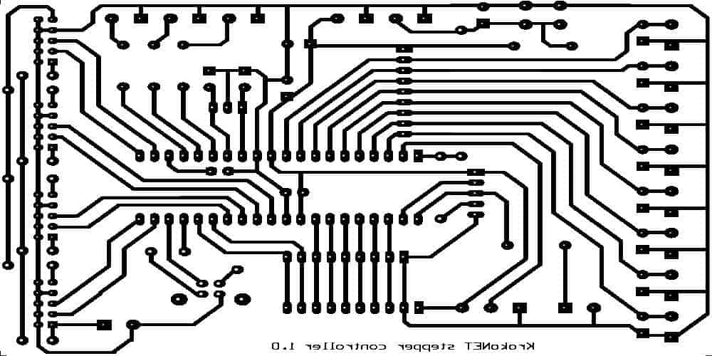
3. Create a Layout for the PCB
We are now going to talk about some of the options available for you when making or creating a layout for the circuit board.
The first point to note is that the layout creation is important, as it allows for the conversion of the circuit schematic chart into the corresponding circuit board layout.
Tools for the PCB Layout
To create the layout, you have two (2) major options. These are the PCB design software (the most popular) and the less-complicated method, such as Microsoft PowerPoint.
If you are considering using a design software, some of the best options are:
4. Get the Printout of the PCB Layout
Now that your circuit design layout is ready, take it out using the laser printer. However, taking out the printout is one of the major places you want to pay extra attention to. Here are some of the things you want to have in mind while at it:
- Glossy Paper Usage: you must use the glossy paper or the magazine paper, if that’s what you are using.
- Go for Black: it is better to have the output or printout of the PCB layout in black. To unify this, consider choosing the color black as the preferred output, both from the circuit board design software and the laser printer drive settings.
- Print on Gloss: the PCB layout’s printout should be made on the glossy or magnificent side of the paper.
5. Cut the Copper Plate
It is now the time to use the copper plate. Note that this has to do with the accurate measurements, so you don’t want to make a wrong cutting pattern.
To get the accurate cutting, you may want to place the PCB layout’s printout on top of the copper plate and then use a cutter or hacksaw to make the pattern.
6. Smoothen It
Now that the copper plate has been cut, it is time to make it smooth. To do this, you must use the abrasive spongy (kitchen) scrub to scrub the side of the circuit board that has been made rough due to cutting.
Besides, scrubbing the sides also helps to remove the picture coating and the top oxide copper layer. You can also use the sanding paper to make the side even smoother – which helps the image to stick better, by the way.
7. Transferring the PCB Printout to the Copper Plate
With the circuit board layout printed and the copper plate smoothened, what’s next is to transfer the layout or the print to the copper plate.
At this point, we will look at the three (3) different methods we mentioned earlier in details:
Using a Permanent Marker
You can transfer the PCB printout to the copper plate, simply by using the permanent market we have on the list of materials.
This method is simpler and can help you make a more manualized process of transferring the PCB prints to the copper plate. You would need both a pencil and the permanent marker for this purpose, whereby the pencil is used to make a sketch of the design on the copper plate. Once the sketch has been made, use the permanent marker to trace over it as a way of making it clearer.
The permanent marker process just explained works best if you are working on either the smaller circuits or the less-complex boards.
Iron Transfer
The method of using iron on glossy paper works best if you are working on complex circuit boards. If that’s the case, here are some of the things you need to know:
- Image Placement: start by transferring the printout of the PCB to the circuit board or copper plate.
- Surface Positioning: the first aspect of positioning the surface is to flip it horizontally. Afterwards, place the surface of the board’s copper on the printed pattern.
- Extra Positioning: you also need to make additional positioning, such as the correct placement of the panel along the edges of the printed pattern. You also want to put a tape or a sheet on the two sides of the board that don’t have coppered sides. That way, the printed layout and the board will be held in shape as you work on them.
With the placements done, here are the steps to take when ironing the PCB print on the board:
- The ironing is done in a way that the side containing the image or print is pressed down to the coppered side.
- Heat up the electric iron to the highest temperature.
- Meanwhile, put the photo paper/image and the board in a way that the back of the print will be facing you. They should be placed on a clean wooden table and with clothes placed underneath.
- Hold one end of the print and place the hot iron at the other end with little pressure for about 15 minutes.
- Apply pressure slowly towards the edge of the board and continue ironing slowly.
- In about 15 minutes, the long pressing of the iron will have melted the ink printed on the glossy paper on the copper plate/board.
- Place the printed plate in lukewarm water and leave for about 10 minutes. This is done both to cool down the heat on the plate and to remove any residue of glossy paper that usually sticks to the board’s surface after the printing or ink transfer.
- It is now time to remove the paper residue. You can start by peeling off at low angles or traces.
- By now, you will see that some of the tracks have been fainted. If so, you will use the permanent marker again to make the traces that are now light in colour.
8. Etch the Printed Plate
Extra care is required here. You are to etch the printed plate by following these steps:
- Wear your rubber or plastic gloves.
- To prevent the etching solution from damaging the floor, consider placing a newspaper or rarely-used cloth beneath the printed plate.
- Fill a plastic box with water and dissolve about 3 teaspoons of the etching solution (ferric chloride solution) inside it.
- Dip the printed plate (PCB) inside the solution and leave it there for about 30 minutes.
- Within this time, the unwanted copper will be removed from the PCB.
- You can now use a pair of pliers to remove the PCB from the solution.
- Check to see if the unmasked area containing the unwanted copper has been fully etched. If it has not, consider putting the PCB back into the solution until the entire (unwanted) copper is etched.
9. Dispose of the Solution
You can now dispose of the etching solution, but make sure not to throw it away in the sink, because it can damage the pipes. You don’t want to throw it into the water, because the solution is toxic to fish and other water-based organisms.
The best way to dispose of the etching solution is to dilute the solution before throwing away somewhere safe – other than the sea or the sink at home.
10. Finalize the Prints
Now, make final touches on the PCB by making a few drops of the thinner (in this case, acetone). Doing this helps to remove any unwanted ink on the PCB’s surface, while making the copper’s surface brighter.
You can then rinse the circuit board and trim to size.
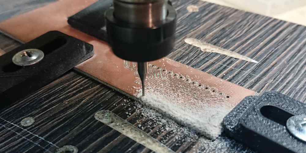
The last steps would be drilling holes on the PCB and soldering all the electronic components needed for the PCB project.
Conclusion
Using the steps in this article, you can print your own Printed Circuit Board (PCB) at home, thereby, saving time, money and most importantly – becoming a near-professional at PCB design and printing.
