After the fabrication of the printed circuit board (PCB), next is the mounting of the electronic components. This is during the standard process of quick turn PCB assembly. The process of advanced assembly PCB deals with some procedures, whereby this personal service has to be followed in the right order so that it functions the right way.
Furthermore, advanced assembly or advanced PCB assembly is known as the last step during PCB manufacturing, which creates an electronic assembly that is functional electronic assembly and integrated in a brand new product.
The electronic devices of today rely on the printed circuit board (PCB) as their main building block. Assuming that the process of quick turn PCB assembly was well executed, then the advanced assembly process is where the product’s true quality will be proven and also created.
Furthermore, PCB design is focused around the placement of the bare board in the advanced assembly process bat any scale levels. This is when the professional designers offer their personal service to ensure that they comprehend the standard steps of processing and its limitations, advanced operational capacity, and advanced assembly.
What are the Processes of Advanced Assembly of Printed Circuit Boards?
Below are the processes of advanced PCB assembly
Stenciling
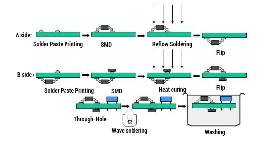
PCB advanced assembly is a step by step process and it is guided. The first ever step in the advanced assembly process is stenciling. Here is the application of the solder paste to the different board sections where you will be mounting the components.
Also, solder paste is composed of small metal balls as well as a substance referred to as flux. In addition, the stenciling is similar to screen-printing. This solder paste is usually applied to a bare PCB making use of a thin stencil made of stainless steel.
Next step is that this stencil is held by a mechanical fixture and the PCB is held in place as the distribution of the solder paste over the stencil takes place. Also, this paste is usually viscous and it stays in specific areas of that bare PCB as soon as you remove the applicator and the stencil.
Automated Placement
The next stage in advanced assembly is component placement making use of the pick and place machine. For through hole technology, the technician has the ability to place any components that some pick and place machines will find too large. Although for high volume advanced assembly in contrast to assembling just a few boards, the process is usually automatic.
Soldering
The securing of the PCB components are done making use of three soldering processes. These include reflow soldering, wave soldering, as well as selective soldering. Just a few boards don’t need reflow soldering and wave soldering. Generally, hand soldering isn’t performed during high volume advanced assembly unless you are performing a rework
Wave soldering is useful during smt assembly and through hole pcb assembly. The standard process utilized for the surface mount advanced assembly is reflow soldering. Two-sided boards have to pass through different cycles of reflow soldering.
Anytime it is used with the hybrid advanced assembly process, it results to a minimum of three solder cycles necessary to assembly your PCB completely.
You complete the reflow soldering through the placing of the components using the pick and place machine. The board is then passed in the reflow oven, which is held close to 250 Celsius. This oven then heats the solder paste up and then makes it to harden to a metal joint on the component pads and pins, which are exposed on the circuit board.
After completing the soldering processes, the advanced assembly takes another step, which is the cleaning of the PCB thoroughly. This could involve using deionized water as well as some cleaning agents in getting out any residues from the PCB surface. This particularly points to the flux residues. Once you are done washing, the PCBs are then dried using compressed air, then you can send the advanced assembly boards for inspection. The board thickness is very important here.
Testing and Inspection
To ensure that the advanced assembly of the PCB is working properly, there is a need to inspect the PCB by doing a test or some tests. With high volume production, this involves more quality assessments to make sure that the whole process is showing effects at low rates.
Once you are done inspecting, some boards may become qualified further with an in-circuit testing. This involves the powering of the board and then probing some points on the advanced assembly of the printed circuit board.
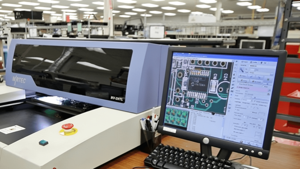
You can perform visual inspection using automated optical inspection. The vision system makes use of high resolution cameras, which you can position at different angles so as to inspect the PCBA’s surface layers. The main goal for this step is to find possible assembly defects, which are related to soldering and components placement. All these include quality of the solder joint, component alignment, components lifting during cooling. You can process large PCB batches quickly using this AOI system.
In addition, for the double sized and single sized PCBs, the AOI becomes a very good inspection tool. However, you cannot use it to examine the inner layers present on the multilayer PCB. Rather you can inspect the multilayer PCBs making use of the X-ray imaging machine.
More on Testing
Professional technicians have the ability to visually inspect the X-ray images. Though newer systems could automate this inspection process via some steps in image processing. When you discover a defect in the X-ray image, then you can flag it for more inspection.
In addition, the X-ray systems are usually used in inspecting BGAs for printed circuit board PCB assembly defects. This includes creation of opens or shorts, and the BGA alignment on the pads.
The processes for testing for finished circuit board or PCB assembly could vary. This depends on the end product’s needs, as well as its reliability level. In addition, the tests go far beyond checks for basic functionality and defect detection to determine the product’s long-term reliability.
Furthermore, depending on whatever standards for quick turn pcb assembly, you may need different testing regimes in the pcb industry.
Conclusion
You can get an advanced assembly circuit board by getting a better personal service from a professional. For large scale production or low volume pcbs, your design engineers must use higher quality metrics to deliver the best.
