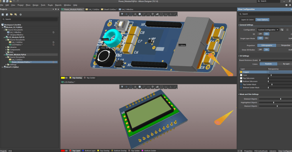
Altium PCB to Schematic is a powerful tool that allows engineers and designers to create and manage printed circuit board (PCB) designs with ease. With this software, users can easily convert their PCB designs into schematics, making it easier to visualize and understand the connections between components.
One of the key benefits of using Altium PCB to Schematic is the ability to streamline the design process. By converting a PCB design into a schematic, engineers can quickly identify any potential issues or errors before moving forward with the manufacturing process. This can save time and money in the long run, as it allows for faster prototyping and reduces the risk of costly mistakes.
Overall, Altium PCB to Schematic is a valuable tool for anyone involved in the design and manufacturing of PCBs. By simplifying the design process and providing a clear visual representation of the connections between components, this software can help to improve efficiency and accuracy, ultimately leading to better quality products.
Altium PCB to Schematic: Overview
What is Altium PCB to Schematic?
Altium PCB to Schematic is a feature that allows users to convert a printed circuit board (PCB) layout into a schematic design. This feature is available in Altium Designer, a popular software tool used for electronic design automation (EDA).
When designing a PCB, it is important to have a corresponding schematic that shows how all the components are connected. Altium PCB to Schematic makes it easier to create this schematic by automatically generating it from the PCB layout.
Why is Altium PCB to Schematic important?
Altium PCB to Schematic is an important feature for several reasons. First, it saves time by eliminating the need to manually create a schematic from scratch. This can be especially useful for complex designs with many components.
Additionally, Altium PCB to Schematic helps ensure accuracy and consistency between the PCB layout and schematic. By automatically generating the schematic from the PCB layout, there is less room for error or discrepancies between the two designs.
Overall, Altium PCB to Schematic is a valuable tool for electronic designers who want to streamline their workflow and ensure accurate and consistent designs.
Note: Altium PCB to Schematic is not a perfect tool and may require some manual adjustments or corrections. It is important to always review the generated schematic to ensure accuracy and completeness.
Altium PCB to Schematic: Steps
Step 1: Open Altium Designer
To begin the process of converting an Altium PCB to a schematic, open Altium Designer and create a new schematic document. Make sure that the schematic document has the same name as the PCB document to ensure a smooth transfer of data.
Step 2: Import the PCB Design
After creating a new schematic document, import the PCB design by going to File > Import > PCB. This will bring up a window that allows you to select the PCB file you want to import. Once you have selected the PCB file, click OK to start the import process.
Step 3: Generate the Schematic
Once the PCB design has been imported, you can generate the schematic by going to Design > Update Schematic From PCB. This will automatically create a schematic based on the PCB design.
It is important to note that the generated schematic will not be perfect and may require some manual adjustments. However, this process can save a lot of time and effort compared to manually creating a schematic from scratch.
In conclusion, converting an Altium PCB to a schematic can be done in just a few simple steps. By following these steps, you can easily generate a schematic based on an existing PCB design.
Altium PCB to Schematic: Tips and Tricks
Useful Shortcuts
When working with Altium PCB to Schematic, there are several useful shortcuts that can help save time and streamline the workflow. Here are a few examples:
Tabkey: Use theTabkey to quickly move between different fields and components on the schematic.Ctrl + CandCtrl + V: Use these shortcuts to copy and paste components or sections of the schematic.Ctrl + Shift + M: This shortcut can be used to quickly move components around the schematic.
Best Practices
To ensure a smooth and efficient workflow when using Altium PCB to Schematic, it is important to follow best practices. Here are a few tips:
- Keep the schematic organized: Use a clear and consistent naming convention for components and nets, and organize them in a logical manner.
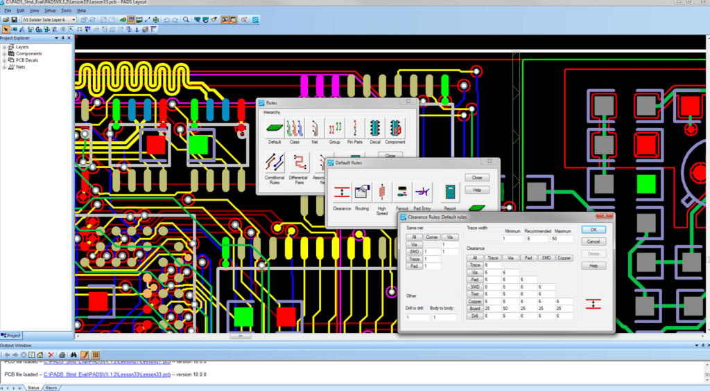
- Use design rules: Set up design rules to ensure that the schematic is error-free and meets the necessary requirements.
- Use hierarchical design: Break up the schematic into smaller, more manageable sections using hierarchical design.
Common Mistakes to Avoid
There are several common mistakes that can be made when working with Altium PCB to Schematic. Here are a few examples:
- Not using the grid: Make sure to use the grid when placing components and nets to ensure that they are aligned properly.
- Not checking for errors: Always double-check the schematic for errors before moving on to the next stage of the design process.
- Not using version control: Use version control to keep track of changes and ensure that the correct version of the schematic is being used.
By following these tips and tricks, you can ensure a smooth and efficient workflow when using Altium PCB to Schematic.
Altium PCB to Schematic: Conclusion

In conclusion, Altium Designer is a powerful software tool that can help you design complex printed circuit boards (PCBs) and schematics. With its intuitive user interface, advanced features, and comprehensive libraries, Altium Designer is a great choice for engineers, designers, and hobbyists who want to create high-quality PCBs and schematics.
One of the key strengths of Altium Designer is its ability to seamlessly integrate PCB and schematic design. This allows you to quickly and easily move between the two, making it easier to design and debug your circuits. Additionally, Altium Designer’s advanced routing capabilities and design rule checking (DRC) tools help ensure that your PCBs are error-free and meet industry standards.
Another advantage of Altium Designer is its extensive library of components and symbols. These libraries include thousands of pre-designed parts, making it easy to find and use the components you need for your designs. Additionally, Altium Designer’s libraries are regularly updated and maintained, ensuring that you always have access to the latest components and symbols.
Overall, Altium Designer is a powerful and versatile tool that can help you design high-quality PCBs and schematics. Whether you’re a professional engineer or a hobbyist, Altium Designer has the features and capabilities you need to bring your designs to life.
