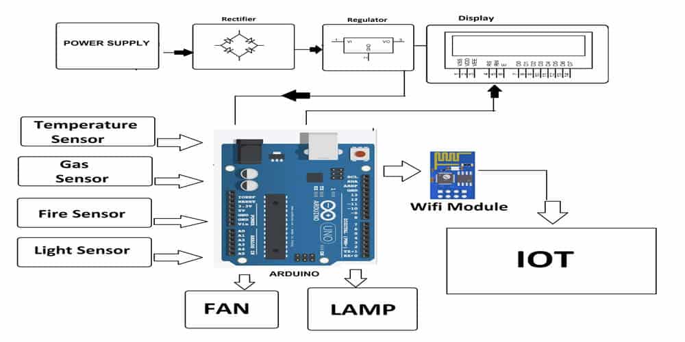
The Arduino Due PCB layout is a crucial component in the development of electronic projects. The Arduino Due is a microcontroller board based on the Atmel SAM3X8E ARM Cortex-M3 CPU. The board contains everything needed to support the microcontroller; simply connect it to a computer with a USB cable or power it with a AC-to-DC adapter or battery to get started.
The PCB layout of the Arduino Due is designed to be user-friendly and easy to navigate. It features a variety of connectors, including a USB host port, a USB device port, an Ethernet jack, and a microSD card slot. The board also includes a reset button, an erase button, and a power LED. With its compact size and versatile design, the Arduino Due is an excellent choice for a wide range of electronic projects.
Overview of Arduino Due PCB Layout
The Arduino Due PCB Layout is designed to provide a solid foundation for building microcontroller-based projects. The board is based on the Atmel SAM3X8E ARM Cortex-M3 CPU, which provides a high-performance computing platform for a wide range of applications. The board has a compact form factor and is easy to use, making it an ideal choice for hobbyists, students, and professionals alike.
Power Supply and Voltage Regulation
The Arduino Due PCB Layout has a robust power supply system that can handle a wide range of input voltages. The board can accept input voltages between 7V and 12V, making it compatible with a variety of power sources. The power supply system includes voltage regulators that provide stable, regulated voltages to the various components on the board. The voltage regulators are designed to handle high current loads, ensuring that the board can deliver reliable power to all of its components.
Clock and Reset Circuitry
The Arduino Due PCB Layout has a precise clock circuit that provides accurate timing for all of the board’s components. The clock circuit is based on a crystal oscillator that provides a stable clock signal to the microcontroller. The board also has a reset circuit that ensures that the microcontroller is properly initialized when the board is powered on or reset.
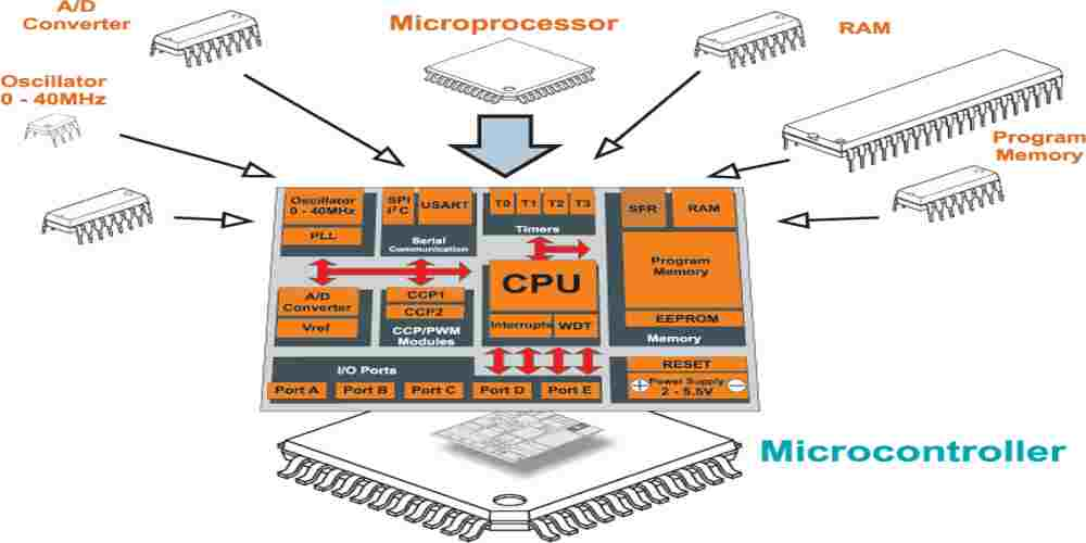
Microcontroller Section
The microcontroller section of the Arduino Due PCB Layout is where the heart of the board lies. The Atmel SAM3X8E microcontroller is mounted on the board and is surrounded by a variety of support components. The microcontroller section includes a USB port that can be used to program the board and to communicate with other devices. The section also includes a variety of input and output pins that can be used to connect the board to other components and devices.
In summary, the Arduino Due PCB Layout is a powerful and versatile board that provides a solid foundation for building microcontroller-based projects. The board’s power supply and voltage regulation system, clock and reset circuitry, and microcontroller section are all designed to provide reliable and accurate performance. Whether you are a hobbyist, student, or professional, the Arduino Due PCB Layout is an excellent choice for your next project.
Designing the Power Supply and Voltage Regulation Circuitry

Choosing the Power Supply Components
Before starting the design of the power supply and voltage regulation circuitry for the Arduino Due PCB, it is important to choose the right components. The power supply components should be able to provide the required voltage and current for the board to function properly. The following components are recommended:
- AC to DC power adapter
- Voltage regulator
- Capacitors
The AC to DC power adapter should have an output voltage of 9V to 12V and a current rating of at least 1A. The voltage regulator should have a maximum input voltage of 20V and a maximum output current of 1.5A. Capacitors should be placed at the input and output of the voltage regulator to filter out noise and stabilize the output voltage.
Schematic Design
The schematic design for the power supply and voltage regulation circuitry should follow the following guidelines:
- Input power should be connected to the input of the voltage regulator through a diode to protect against reverse polarity.
- Capacitors should be placed at the input and output of the voltage regulator.
- The output of the voltage regulator should be connected to the 5V and 3.3V rails of the Arduino Due.
- A fuse should be placed in series with the input power to protect against overcurrent.
PCB Layout Design
The PCB layout design for the power supply and voltage regulation circuitry should follow the following guidelines:
- The input power connector should be placed near the edge of the board for easy access.
- The voltage regulator and capacitors should be placed close to each other to minimize trace length and reduce noise.
- The 5V and 3.3V rails should be routed to the appropriate connectors on the board.
By following these guidelines, the power supply and voltage regulation circuitry for the Arduino Due PCB can be designed to provide stable and reliable power to the board.
Designing the Clock and Reset Circuitry
Choosing the Clock and Reset Components
The clock and reset circuitry is a crucial part of any microcontroller-based design. For the Arduino Due board, the clock and reset circuitry must be designed to meet the requirements of the Atmel SAM3X8E microcontroller. The clock must be stable and accurate, and the reset circuitry must be reliable and robust.
When choosing the clock and reset components, it is important to consider the requirements of the microcontroller and the overall design goals. For the Arduino Due board, a crystal oscillator is used as the clock source, and a simple RC circuit is used for the reset circuit.
Schematic Design
The clock and reset circuitry can be designed using a schematic editor. The schematic should include the crystal oscillator, capacitors, resistors, and the reset circuitry components. The schematic should be designed to meet the requirements of the microcontroller and the overall design goals.
In the schematic, the crystal oscillator should be connected to the microcontroller’s clock input pins, and the capacitors should be connected to the crystal oscillator to stabilize the clock signal. The reset circuitry should be connected to the microcontroller’s reset input pin, and should include the necessary components to ensure reliable and robust operation.
PCB Layout Design
The clock and reset circuitry should be laid out on the PCB to minimize noise and interference. The crystal oscillator and capacitors should be placed close to the microcontroller’s clock input pins, and the reset circuitry should be placed close to the microcontroller’s reset input pin.
The PCB layout should also include ground and power planes to minimize noise and interference. The ground and power planes should be connected to the microcontroller’s ground and power pins, respectively.
In summary, designing the clock and reset circuitry for the Arduino Due board requires careful consideration of the microcontroller’s requirements and the overall design goals. The clock and reset components should be chosen to meet these requirements, and the schematic and PCB layout should be designed to ensure reliable and robust operation.
Designing the Microcontroller Section
Choosing the Microcontroller and Supporting Components
The first step in designing the microcontroller section is to choose the appropriate microcontroller and supporting components. The Arduino Due uses the Atmel SAM3X8E microcontroller, which is a 32-bit ARM Cortex-M3 processor. In addition to the microcontroller, the supporting components include voltage regulators, crystal oscillators, capacitors, and resistors.
When selecting the microcontroller, it is important to consider the required features and performance specifications. The SAM3X8E is a good choice for the Arduino Due because it has a high clock speed, a large amount of flash memory, and many peripherals. The supporting components must be carefully chosen to ensure that they meet the specifications of the microcontroller and the overall system.
Schematic Design
Once the microcontroller and supporting components have been selected, the next step is to design the schematic. The schematic is a diagram that shows the connections between the various components in the circuit. The schematic must be carefully designed to ensure that all of the components are connected correctly and that the circuit functions as intended.
The schematic design should include all of the required components, including the microcontroller, voltage regulators, crystal oscillators, capacitors, and resistors. It is important to follow the datasheets for each component and to ensure that the circuit meets the specifications of the microcontroller and the overall system.
PCB Layout Design
After the schematic has been designed and verified, the next step is to design the PCB layout. The PCB layout is the physical layout of the components on the printed circuit board. The PCB layout must be carefully designed to ensure that all of the components fit on the board and that the board functions as intended.
The PCB layout design should include all of the required components, including the microcontroller, voltage regulators, crystal oscillators, capacitors, and resistors. It is important to follow the design rules for the PCB manufacturer and to ensure that the layout meets the specifications of the microcontroller and the overall system.
In summary, designing the microcontroller section of the Arduino Due requires careful selection of the microcontroller and supporting components, schematic design, and PCB layout design. By following these steps, a functional and reliable microcontroller section can be designed for the Arduino Due.
